
资料下载


了解单片机内部总线结构如何驱动应用效率
分享资料个
了解单片机内部总线结构如何驱动应用效率
MCU的片上外设,现在可以同时使用,从CPU负载低级别的功能,一个惊人的数字。这可以大大提高处理效率,降低功耗,简化您的设计。然而,如果你的外围功能压倒了内部总线接口和数据传输速度急剧下降,你可能会有一个不幸的惊喜。幸运的是,MCU制造商增加了新的和高效的总线接口,往往与多个关键外设和片上存储器之间的路径,可以帮助支持多个数据传输。然而,这些新的巴士有限制,因为连接一切到其他一切是太昂贵的模具面积和功率。了解这些新的片上总线的通用模型将帮助您创建高效的设计,最大限度地提高数据传输带宽。
本文将快速回顾一些常见的智能片上总线功能,并将说明示例设计,利用这些关键功能。所涉及的主题包括:片上总线矩阵结构,DMA控制器的使用,专用外设数据传输功能,智能缓冲,总线优先系统和中断控制。
Common bus-interface architectures
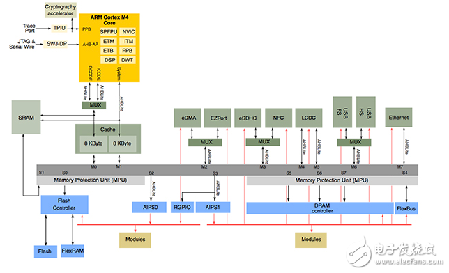
Several key architectural approaches show up in just about every high-performance bus-interconnect structure. This should not be surprising since the key strategy to supporting high bandwidth is to be able to establish several parallel connections that can run independently. A bus-matrix architecture, where several bus masters can independently access several bus slaves, is perhaps the most common building block for high-efficiency bus architectures. The Freescale Kinetis K70 MCU is a good example of the type of interconnect architecture required for efficient data processing and movement.
As shown in Figure 1, the Freescale Kinetis K70 MCU uses a multilevel bus matrix that can interconnect between eight separate bus masters and eight separate bus slaves. It is possible for multiple masters and slaves to operate independently. Allocation of memory is critical to maximize efficiency. For example, the following operations could all operate in parallel with no overlap:
Core - instructions in Flash and core only data and stack in SRAM_L
USB - data buffers in SRAM_U
LCD controller - graphic buffers in DDR

声明:本文内容及配图由入驻作者撰写或者入驻合作网站授权转载。文章观点仅代表作者本人,不代表电子发烧友网立场。文章及其配图仅供工程师学习之用,如有内容侵权或者其他违规问题,请联系本站处理。 举报投诉
- 相关下载
- 相关文章


