
资料下载


ADuC814单片机®小封装的12位ADC与嵌入式闪存微程序控制器
分享资料个
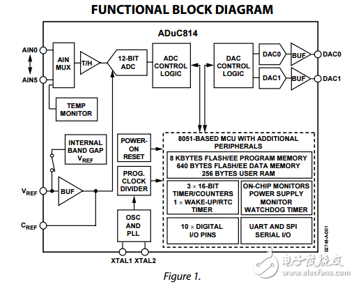
The ADuC814 is a fully integrated 247 kSPS, 12-bit data acquisition system incorporating a high performance multichannel ADC, an 8-bit MCU, and program/data Flash/EE memory on a single chip. This low power device operates from a 32 kHz crystal with an on-chip PLL generating a high frequency clock of 16.78 MHz. This clock is, in turn, routed through a programmable clock divider from which the MCU core clock operating frequency is generated. The microcontroller core is an 8052 and is compatible with an 8051 instruction. 8 kBytes of nonvolatile Flash/EE program memory are provided on-chip. 640 bytes of nonvolatile Flash/EE data memory and 256 bytes RAM are also integrated on-chip. The ADuC814 also incorporates additional analog functionality with dual 12-bit DACs, a power supply monitor, and a band gap reference. On-chip digital peripherals include a watchdog timer, time interval counter, three timer/counters, and two serial I/O ports (SPI and UART)。 On-chip factory firmware supports in-circuit serial download and debug modes (via UART), as well as single-pin emulation mode via the DLOAD pin. The ADuC814 is supported by a QuickStart™ Development System. The part operates from a single 3 V or 5 V supply over the extended temperature range −40°C to +125°C. When operating from 3 V supplies, the power dissipation for the part is below 10 mW. The ADuC814 is housed in a 28-lead TSSOP package.
声明:本文内容及配图由入驻作者撰写或者入驻合作网站授权转载。文章观点仅代表作者本人,不代表电子发烧友网立场。文章及其配图仅供工程师学习之用,如有内容侵权或者其他违规问题,请联系本站处理。 举报投诉
- 相关下载
- 相关文章


