

ADC16V130功能特性以及应用的介绍
RF/无线
描述
NS 公司的ADC16V130是LVDS输出的16位130MSPS高性能ADC,双电源1.8V和3.0V工作,16位分辨率,取样速率130MSPS,满功率带宽1.4GHz,160-MHz的SNR为76.7dB, SFDR为90.6dBFS,主要应用在高IF取样接收器,多载波基站接收器,测试测量设备,通信基础设备,数据采集和手提仪表等.本文介绍了ADC16V130主要特性,方框图,低频和高频变压器驱动电路以及SP16130CH4RB低IF接收器参考设计主要特性,详细电路图和材料清单(BOM).
ADC16V130: 16-Bit, 130 MSPS A/D Converter with LVDS Outputs
The ADC16V130 is a monolithic high performance CMOS analog-to-digital converter capable of converting analog input signals into 16-bit digital words at rates up to 130 Mega Samples Per Second (MSPS). This converter uses a differential, pipelined architecture with digital error correction and an onchip sample-and-hold circuit to minimize power consumption and external component count while providing excellent dynamic performance. Automatic power-up calibration enables excellent dynamic performance and reduces part-to-part variation, and the ADC16V130 could be re-calibrated at any time by asserting and then de-asserting power-down. An integrated low noise and stable voltage reference and differential reference buffer amplifier easies board level design. On-chip duty cycle stabilizer with low additive jitter allows wide duty cycle range of input clock without compromising its dynamic performance. A unique sample-and-hold stage yields a fullpower bandwidth of 1.4 GHz. The digital data is provided via full data rate LVDS outputs – making possible the 64-pin, 9mm x 9mm LLP package. The ADC16V130 operates on dual power supplies +1.8V and +3.0V with a power-down feature to reduce the power consumption to very low levels while allowing fast recovery to full operation.
ADC16V130主要特性:
■ Dual Supplies: 1.8V and 3.0V operation
■ On chip automatic calibration during power-up
■ Low power consumption
■ Multi-level multi-function pins for CLK/DF and PD
■ Power-down and sleep modes
■ On chip precision reference and sample-and-hold circuit
■ On chip low jitter duty-cycle stabilizer
■ Full data rate LVDS output port
■ 64-pin LLP package (9x9x0.8, 0.5mm pin-pitch)
ADC16V130主要指标:
■ Resolution 16 Bits
■ Conversion Rate 130 MSPS
■ SNR
(fIN = 10MHz)
(fIN = 70MHz)
(fIN = 160MHz)
78.5 dBFS (typ)
77.8 dBFS (typ)
76.7 dBFS (typ)
■ SFDR
(fIN = 10 MHz)
(fIN = 70MHz)
(fIN = 160MHz)
95.5 dBFS (typ)
92.0 dBFS (typ)
90.6 dBFS (typ)
■ Full Power Bandwidth 1.4 GHz (typ)
■ Power Consumption
Core
LVDS Driver
Total
650 mW (typ)
105 mW (typ)
755 mW (typ)
■ Operating Temperature Range -40°C ~ 85°C
ADC16V130应用:
■ High IF Sampling Receivers
■ Multi-carrier Base Station Receivers GSM/EDGE, CDMA2000, UMTS, LTE and WiMax
■ Test and Measurement Equipment
■ Communications Instrumentation
■ Data Acquisition
■ Portable Instrumentation
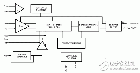
图1.ADC16V130方框图
图2. ADC16V130低频输入变压器驱动电路
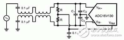
图3. ADC16V130高频输入变压器驱动电路
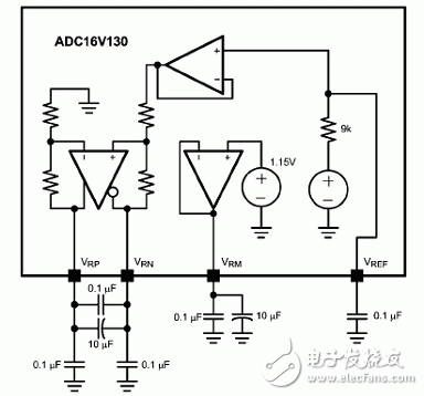
图4. ADC16V130内部基准和去耦电路
SP16130CH4RB参考设计板
The SP16130CH4RB Reference Board demonstrates a low IF receiver subsystem application including an ADC16V130 analog-to-digital converter (ADC) and LMK04031B clock conditioner which provides digitization and clocking as used in wireless infrastructure systems.
This subsystem reference design provides single to differential conversion and lowpass filtering of the input signal with an optimized, double-balun network and high dynamic range digitization to parallel LVDS outputs using the ADC16V130. The 125 MHz low-jitter, LVPECL clock signal for the ADC is generated by a LMK04031B clock conditioner which demonstrates less than 250 fs of total jitter over the input bandwidth of the ADC.
The measured system performance demonstrates a large signal SNR of 75.8 dBFS and SFDR greater than 84 dBFS for a -1 dBFS, 52 MHz input signal and a sampling frequency of 125 MSPS. For small signals, the performance improves to 78.0 dBFS SNR and greater than 94 dBFS SFDR.
Evaluation of this reference board is simplified with the WaveVision 5.1 Data Capture Board and WaveVision 5 software.
SP16130CH4RB低IF接收器参考设计板主要特性:
Key Features of the SP16130CH4RB Low IF Receiver Reference Design Board
■ Demonstrates a subsystem architecture used in wireless infrastructure systems and
frequency domain analyzers
■ Configured for input frequencies between 5 and 52 MHz
■ Board comes fully assembled and tested
■ Single (+5V) supply needed
■ All ADC features can be exercised
■ Featured Products Include:
— ADC16V130 16-bit, 130 Megasample per second (MSPS) ADC with parallel LVDS outputs
— LMK04031B low-jitter precision clock conditioner consisting of cascaded phase locked loops (PLLs), an internal voltage controlled oscillator (VCO) and a distribution stage
— Several energy-efficient power management ICs
■ Large-signal (-1 dBFS) performance for a 52 MHz input signal:
— SNR = 75.8 dBFS
— SFDR > 84 dBFS
■ Small-signal (-20 dBFS) performance for a 52 MHz input signal:
— SNR = 78.0 dBFS
— SFDR > 94 dBFS
■ Total integrated jitter < 250 fs
■ PIC Loader board included with reference board for quick and easy configuration of the LMK04031B
■ Compatible with the WaveVision 5.1 Data Capture Board and WaveVision 5 software for simplified evaluation
图5.低IF接收器参考设计板外形图
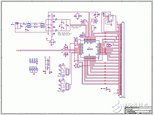
图6.SP16130CH4RB电路图: ADC
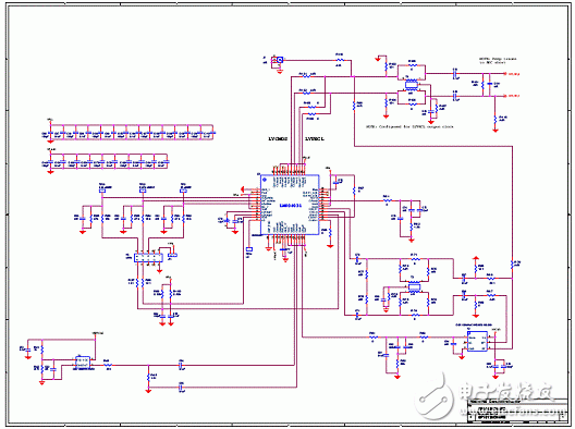
图7.SP16130CH4RB电路图: LMK
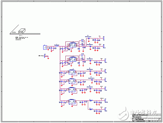
图8SP16130CH4RB电路图:电源
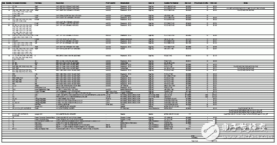
8SP16130CH4RB材料清单:
-
AD7722 16位Σ - ∆ ADC:特性、应用与设计要点2026-04-03 170
-
16位130 MSPS IF采样ADC AD9461:高性能数据转换的理想选择2026-04-02 511
-
深入剖析LTC2358 - 16:高性能16位ADC的卓越特性与应用2026-03-27 259
-
深度解析AMC130M03:高精度三通道ADC的卓越之选2026-01-20 570
-
ADC16V130 16位130-MSPS模数转换器技术文档总结2025-11-24 711
-
AMC130M02 隔离式 ΔΣ ADC 技术总结2025-10-28 953
-
隔离式高精度ADC AMC130M02在电力计量中的应用2025-08-12 1259
-
ADC16V130 16位、130 MSPS模数转换器数据表2024-07-23 588
-
简述stm32的adc系统的功能特性2021-08-05 3006
-
设计解决方案44-高灵敏度接收器应用受益于16位130 Msps ADC的独特功能2021-05-16 841
-
LTC2208:16位、130 Msps ADC数据表2021-05-10 921
-
AD9461:16位、130 MSPS IF采样ADC数据表2021-04-27 823
-
高灵敏度接收器应用受益于16位130Msps ADC的独特功能2019-09-11 1343
全部0条评论

快来发表一下你的评论吧 !
