

Linear 105V 2.3A低EMI降压稳压器解决方案--LTC7103介绍
电源/新能源
描述
Linear公司的LTC7103是采采用恒频平均电流模式控制架构的高效单片同步降压DC/DC转换器,输入电压从4.4V到105V,可调输出电压从1V到VIN,输出电流高达2.3A.具有超低EMI/EMC,CISPR 25兼容,100%最大占空比工作,可编固定频率200kHz-2MHz.主要用在电池充电器和CC/CV电源,汽车和军用系统,工业,航空和重型设备以及医疗设备和通信系统.本文介绍了LTC7103主要特性,框图和多种应用电路,以及演示板DC2317A,电路图和材料清单.
The LTCR7103 is a high efficiency, monolithic synchronousstep-down DC/DC converter utilizing a constant frequency,average current mode control architecture. It operates from an input voltage range of 4.4V to 105V and provides anadjustable regulated output voltage from 1V to VIN whiledelivering up to 2.3A of output current.
The LTC7103 features high frequency operation anda low minimum on-time that reduce inductor size andenable constant-frequency operation even at very highstep-down ratios. In addition, the LTC7103 achieves thelowest possible dropout voltage with 100% maximumduty cycle operation. During light load operation, converterefficiency and output ripple can be optimized by selectingBurst Mode or pulse-skipping operation.
The LTC7103 includes accurate, high speed average currentprogramming and monitoring without the need foran external sense resistor. Additional features include a bypass LDO to maximize efficiency, fixed or adjustableoutput voltage and loop compensation, and a wide arrayof protection features to enhance reliability.
LTC7103主要特性:
Wide VIN Range: 4.4V to 105V (110V Abs Max)
Ultralow EMI/EMC Emissions: CISPR 25 Compliant
2μA IQ When Regulating 48VIN to 3.3VOUT
Fast and Accurate Output Current Programming andMonitoring with No External RSENSE
Brick Wall Current Limit
Low Minimum On-Time: 40ns
Wide VOUT Range: 1V to VIN
100% Maximum Duty Cycle Operation
Programmable Fixed Frequency: 200kHz to 2MHz
Eight, Pin-Selectable Fixed (1.2V to 15V) orAdjustable Output Voltages
Selectable Pulse-Skipping or Low Ripple BurstModeR Operation at Light Loads
PLL Synchronization to External Clock
EXTVCC LDO Powers Chip from VOUT = 3.3V to 40V
OPTI-LOOPR or Fixed Internal Compensation
Input and Output Overvoltage Protection
Thermally Enhanced (5mm × 6mm) QFN Package
LTC7103应用:
Battery Chargers and CC/CV Supplies
Automotive and Military Systems
Industrial, Avionics and Heavy Equipment
Medical Instruments and TelecommunicationSystems
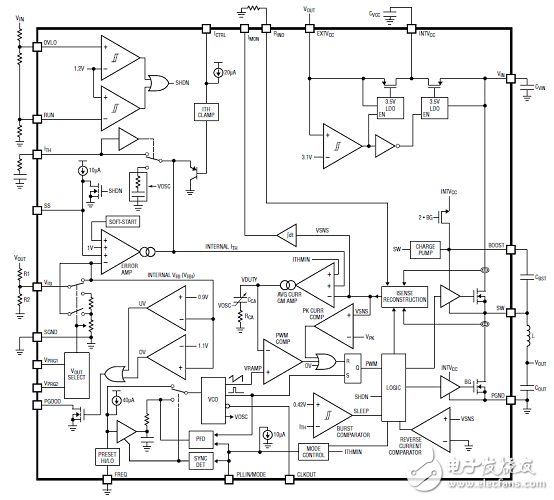
图1.LTC7103框图
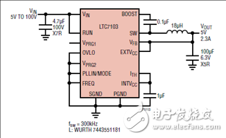
图2.LTC7103应用电路:高效5V-100V输入,5V/2.3A输出
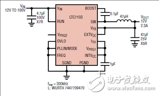
图3.LTC7103应用电路:高效12V-100V输入,12V/2.3A输出
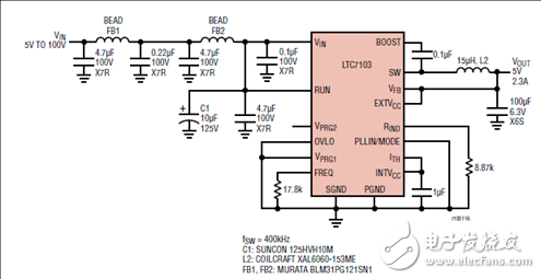
图4.LTC7103应用电路:低EMI 5V-100V输入,5V/2.3A输出
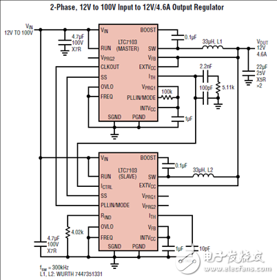
图5.LTC7103应用电路:2相,12V-100V输入,12V/4.6A输出
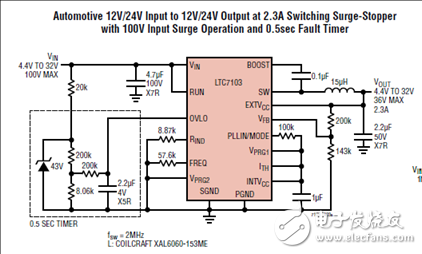
图6.LTC7103应用电路:汽车12V/24V输入,12V/24V 2.3A输出,100V输入浪涌,0.5秒故障计时器
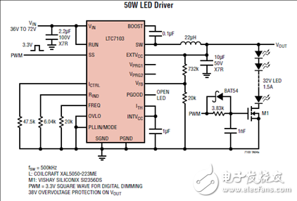
图7.LTC7103应用电路:50W LED驱动器
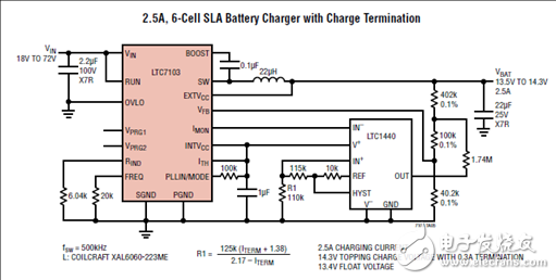
图8.LTC7103应用电路:带充电终止的2.5A 6颗SLA电池充电器
演示板DC2317A
Demonstration circuit 2317A is a 100V monolithic DC/DC step-down regulator featuring the LTC®7103. Thedemo board is designed for a 5V/2.3A output from a 5Vto 100V input at 400kHz switching frequency. The wideinput range makes it suitable for automotive, industrial,medical instrument, and telecom applications. This buckregulator has a peak efficiency of 93.5% at 12VIN, 88.3%at 48VIN and 81.5% at 100VIN.
The LTC7103 is a compact, high efficiency synchronousmonolithic step-down switching regulator with fast currentprogramming. The power switches, compensationnetwork and other necessary circuits are inside of theLTC7103 to minimize external components and simplifydesign. The LTC7103 has wide operating range from 4.4Vto 105V. A 40ns minimum on-time, together with 100%maximum duty cycle allow practical use at any output voltagebetween 1V and VIN. The switching frequency can beprogrammed either via an oscillator resistor or an externalclock over a 200kHz to 2MHz range. Additional featuresinclude a fast and accurate output current programmingand monitoring, and ultralow EMI/EMC emissions.
The demo board has an EMI filter installed. The EMIperformance of the board (with EMI filter) is shown inFigure 2. The figure shows that the circuit passes theCISPR 25 radiated emission test with a wide margin. Toachieve EMI/EMC performance as shown in Figure 2, theinput EMI filter is required and the input voltage shouldbe applied at +VIN_EMI turret pin.The demo board provides current monitor and outputclock signal to interface with an external application circuit.
User selectable mode selection (JP1) is provided andBurst Mode® operation position is selected by default.Burst Mode operation increases light load efficiency whilepulse-skipping mode allows constant-frequency operationto a lighter load. This demo board allows phase-lockedloop (PLL) synchronization to an external clock by selecting SYNC mode on JP1 and by providing a clock signalon CLKIN turret.
The LTC7103 data sheet gives a complete description ofthe part, operation and application information. The datasheet must be read in conjunction with this demo manualfor DC2317A. The LTC7103 is assembled in the 36 (26)lead QFN package. Proper board layout is essential formaximum thermal and electrical performance. See the data sheet sections for details.
图9.演示板DC2317A外形图
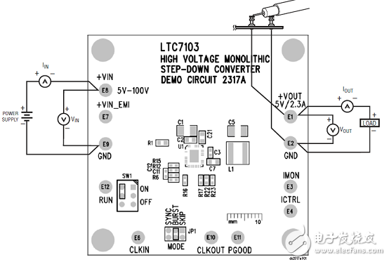
图10.演示板DC2317A测量建立图
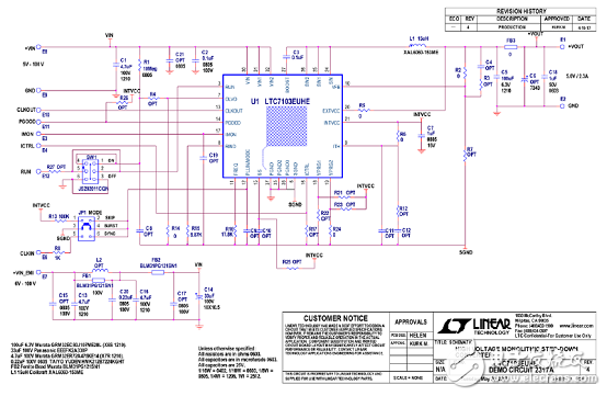
图11.演示板DC2317A电路图
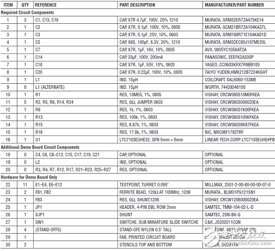
演示板DC2317A材料清单:
-
LTM4707 µModule稳压器LINEAR2025-02-27 4204
-
LTC7103很容易烧掉为什么2026-05-25 12
-
42V,2A / 3A峰值同步降压稳压器,具有2.5μa静态电流和超低EMI辐射2018-09-13 3236
-
Linear LT3509双路36V降压开关稳压器应用方案2009-11-09 1789
-
Linear推出1.2A、55V 降压型开关稳压器2009-11-25 737
-
105V、2.3A、低 EMI 同步降压型稳压器2018-06-04 5675
-
介绍 LTC7103 的特点性能与应用2018-06-28 4719
-
LTC7103 105V、2.3A、低 EMI、同步降压型稳压器2019-02-22 463
-
低EMI同步降压稳压器LTC7103的性能特点分析2019-08-28 3286
-
LTC7103: 105V, 2.3A Low EMI Synchronous Step-Down Regulator Data Sheet2021-01-28 933
-
LTC7103 Demo Circuit - High Efficiency, Low EMI Step-Down Regulator (5-100V to 5V @ 2.3A)2021-02-04 890
-
开关稳压器的 EMI 解决方案2021-03-21 976
-
LT7101:105V、1A快速电流编程低EMI同步降压稳压器2021-05-13 792
-
LTC3412A项目-3A,4 MHz,单片降压稳压器(2.3-5.5V至1.8V@3A)2021-05-31 1378
-
LTC7103演示电路-高效率、低EMI降压稳压器(5-100V至5V@2.3A)2021-06-01 1000
全部0条评论

快来发表一下你的评论吧 !
