

Silabs 评估板Si5332-12EX-EVB PCB设计图解
PCB
描述
Silabs公司的Si5332是低功耗6/8/12路输出可编时钟发生器,采用灵活的频率合成技术,可产生具有极好抖动性能(230 fs rms)的任何组合的输出频率,差分输出频率5-312.5MHz, LVCMOS输出频率5-170MHz,每个输出格式为LVDS, LVPECL, HCSL,LVCMOS,工作温度–40 到 +85℃,主要用在服务器,存储器和搜索加速器,以太网交换和路由器,打印图像,通信,广播视频,测试测量以及小型蜂窝,移动网络.本文介绍了Si5332主要特性,6/8/12路输出功能框图,以及评估板Si5332-12EX-EVB框图和电路图,材料清单和PCB设计图.
Highly Integrated, Low-Power Clock ICs from Silicon Labs Simplify Timing for Demanding 10/25/100G DesignsBased on Silicon Labs proprietary MultiSynth™ flexible frequency synthesis technology,the Si5332 generates any combination of output frequencies with excellent jitter performance(230 fs rms). The device ’s highly flexible architecture enables a single device togenerate a wide range of integer and non-integer related frequencies on up to 12 differentialclock outputs with 0 ppm frequency synthesis error. The device offers multiplebanks of outputs that can each be tied to independent voltages, enabling usage in mixed-supply applications. Further, the signal format of each clock output is user-configurable.
Given its frequency, format, and supply voltage flexibility, the Si5332 is ideallysuited to replace multiple clock ICs and oscillators with a single device.The Si5332 is quickly and easily configured using ClockBuilder Pro™ software. Clock-Builder Pro assigns a custom part number for each unique configuration. Devicesordered with custom part numbers are factory-programmed free of charge, making iteasy to get a custom clock uniquely tailored for each application. Si5332 can also beprogrammed via an I2C serial interface.
The Si5332 is a high-performance, low-jitter clock generator capable of synthesizing up to twelve user-programmable clock frequenciesup to 312.5 MHz. The device supports free run operation using an external or embedded crystal, or it can lock to an external clocksignal. The output drivers support up to twelve differential clocks or twenty four LVCMOS clocks, or a combination of both. The outputdrivers are configurable to support common signal formats, such as LVPECL, LVDS, HCSL, and LVCMOS. VDDO pins are provided forversatility, which can be set to 3.3 V, 2.5 V, 1.8 V or 1.5 V (CMOS only) to power the multi-format output drivers. The core voltagesupply (VDD) accepts 3.3 V, 2.5 V, or 1.8 V and is independent from the output supplies (VDDOxs). Using its two-stage synthesis architectureand patented high-resolution low-jitter MultiSynth technology, the Si5332 can generate an entire clock tree from a single device.
The Si5332 combines a wideband PLL with next generation MultiSynth technology to offer the industry’s highest output count high performanceprogrammable clock generator, while maintaining a jitter performance of 230 fs RMS. The PLL locks to either an external 16-50 MHz crystal or an embedded 50 MHz crystal for generating for generating free-running clocks or to an external clock (CLKIN_2/CLKIN_2# or CLKIN_3/CLKIN_3#) for generating synchronous clocks. In free-run mode, the oscillator frequency is multiplied by thePLL and then divided down either by an integer divider or MultiSynth for fractional synthesis.
The Si5332 features user-defined universal hardware input pins which can be configured in the ClockBuilder Pro software utility. Universalhardware pins can be used for OE, spread spectrum enable, input clock selection, output frequency selection, or I2C address select. If additional hardware input pins are needed, a user can define a different clock output as universal hardware input pins insteadusing ClockBuilder Pro.
The device provides the option of storing a user-defined clock configuration in its non-volatile memory (NVM), which becomes the defaultclock configuration at power-up. To enable in-system programming, a power up mode is available through OTP which powers upthe chip in an OTP defined default mode but with no outputs enabled. This allows a host processor to first write a user defined subset ofthe registers and then restart the power-up sequence to activate the newly programmed configuration without re-downloading the OTP.
Si5332主要特性:
• Any-Frequency 6/8/12-outputprogrammable clock generators
• Offered in three different package sizes,supporting different combinations of output
clocks and user configurable hardwareinput pins
• 32-pin QFN, up to 6 outputs
• 40-pin QFN, up to 8 outputs
• 48-pin QFN, up to 12 outputs
• MultiSynth technology enables anyfrequencysynthesis on any output up to250 MHz
• Highly configurable output path featuring across point mux
• Up to three independent fractionalsynthesis output paths
• Up to five independent integer dividers
• Embedded 50 MHz crystal option
• Input frequency range:
• External crystal: 16 to 50 MHz
• Differential clock: 10 to 250 MHz
• LVCMOS clock: 10 to 170 MHz
• Output frequency range:
• Differential: 5 to 312.5 MHz
• LVCMOS: 5 to 170 MHz
• User-configurable clock output signalformat per output: LVDS, LVPECL, HCSL,LVCMOS
• Temperature range: –40 to +85℃
• Down and center spread spectrum
• Pb-free, RoHS-6 compliant
• Si5332 Family Reference Manual
Si5332应用:
• Servers, Storage, Search Acceleration
• Ethernet Switches, Routers
• Small Cells, Mobile Backhaul/Fronthaul
• Print Imaging
• Communications
• Broadcast Video
• Test and Measurement
• Industrial, Embedded Computing
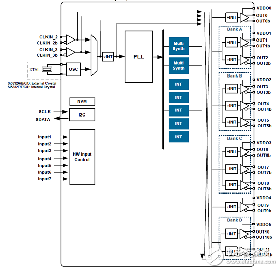
图1.12输出48-QFN封装Si5332框图
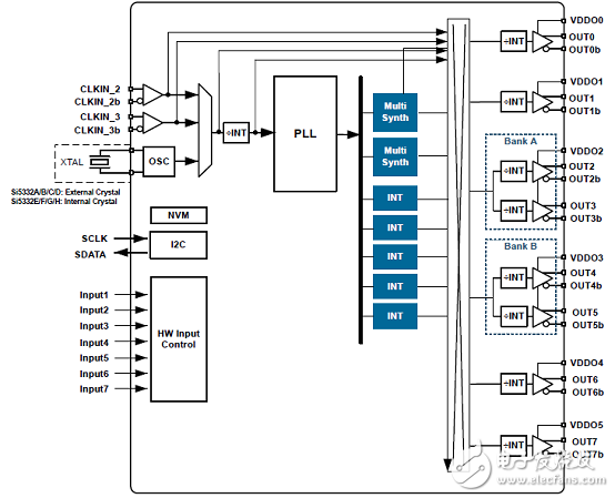
图2.8输出40-QFN封装Si5332框图
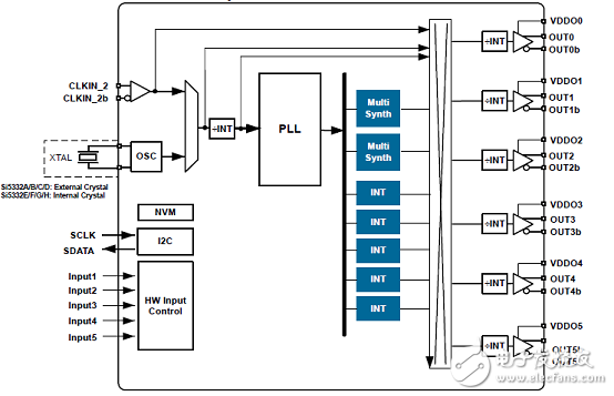
图3.6输出32-QFN封装Si5332框图
评估板Si5332-12EX-EVB
The Si5332-12EX-EVB is used for evaluating the Si5332 Low Jitter Any-Frequency Clock Generator. The Si5332 uses the patented Multisynth™ technology to generate up to twelve independent clock frequencies each with 0 ppm synthesis error. TheSi5332-12EX-EVB has three independentinput clocks. The Si5332-12EX-EVB can be controlled and configured using the ClockBuilder Pro™ (CB Pro™) software tool.
评估板Si5332-12EX-EVB主要特性:
• Powered from USB port or external powersupply.
• Onboard 25 MHz XTAL allows free-runmode of operation on the Si5332 or up to 2input clocks for synchronous clocking.
• CBPro™ GUI programmable VDD supplyallows device to operate from 3.3, 2.5, or1.8 V.
• CBPro GUI programmable VDDO suppliesallow each of the 10 outputs to have itsown power supply voltage selectable from3.3, 2.5, or 1.8 V.
• CBPro GUI-controlled voltage, current, andpower measurements of VDD and allVDDO supplies.
• SMA connectors for input and outputclocks.
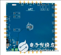
图4.评估板Si5332-12EX-EVB外形图
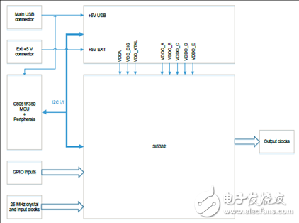
图5.评估板Si5332-12EX-EVB功能框图
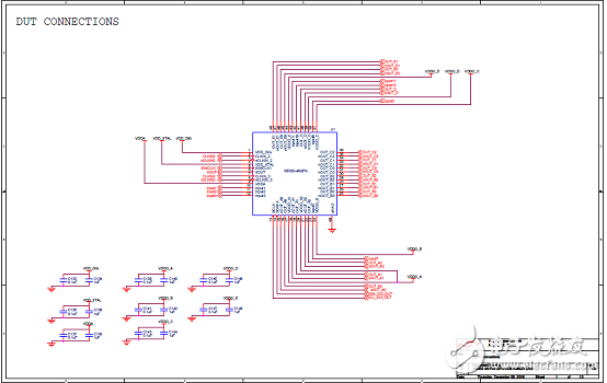
图6.评估板Si5332-12EX-EVB电路图(1)
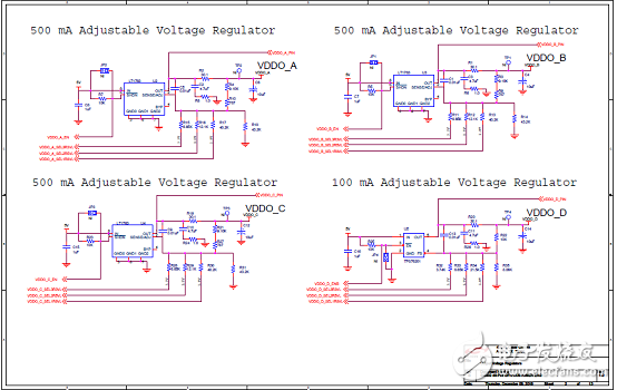
图7.评估板Si5332-12EX-EVB电路图(2)
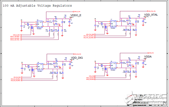
图8.评估板Si5332-12EX-EVB电路图(3)
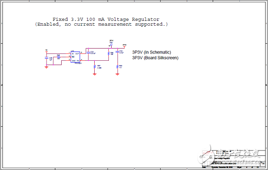
图9.评估板Si5332-12EX-EVB电路图(4)
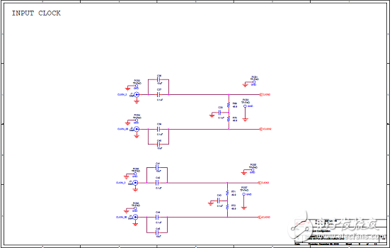
图10.评估板Si5332-12EX-EVB电路图(5)
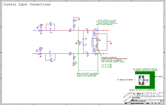
图11.评估板Si5332-12EX-EVB电路图(6)
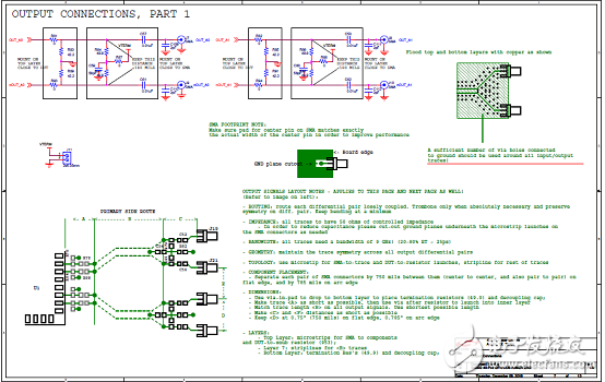
图12.评估板Si5332-12EX-EVB电路图(7)
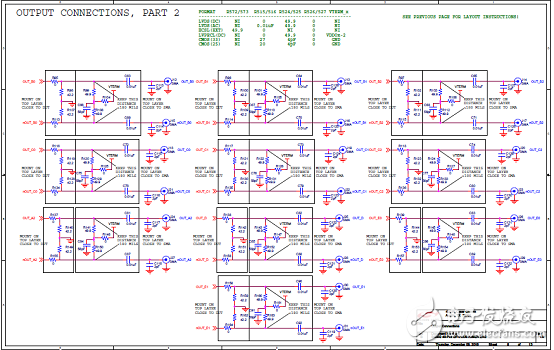
图13.评估板Si5332-12EX-EVB电路图(8)
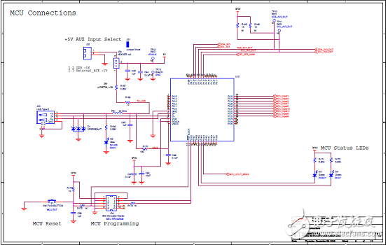
图14.评估板Si5332-12EX-EVB电路图(9)
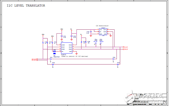
图15.评估板Si5332-12EX-EVB电路图(10)
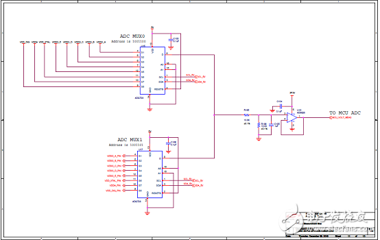
图16.评估板Si5332-12EX-EVB电路图(11)
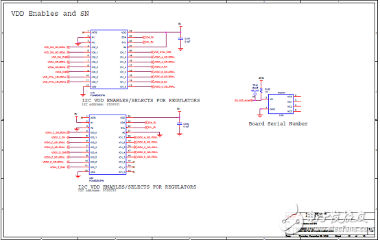
图17.评估板Si5332-12EX-EVB电路图(12)
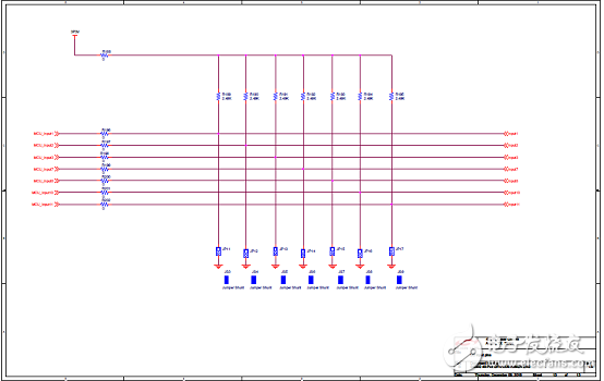
图18.评估板Si5332-12EX-EVB电路图(13)
评估板Si5332-12EX-EVB材料清单:
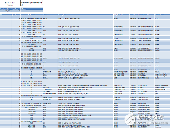
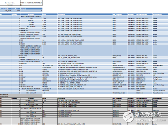

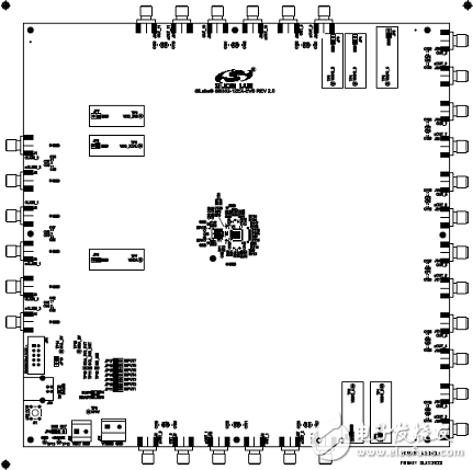
图19.评估板Si5332-12EX-EVB PCB设计图(1)

图20.评估板Si5332-12EX-EVB PCB设计图(2)

图21.评估板Si5332-12EX-EVB PCB设计图(3)
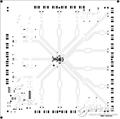
图22.评估板Si5332-12EX-EVB PCB设计图(4)
图23.评估板Si5332-12EX-EVB PCB设计图(5)
图24.评估板Si5332-12EX-EVB PCB设计图(6)

图25.评估板Si5332-12EX-EVB PCB设计图(7)
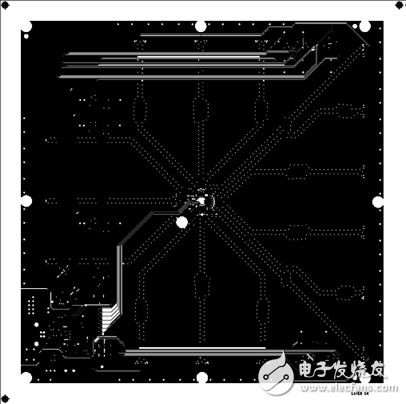
图26.评估板Si5332-12EX-EVB PCB设计图(8)
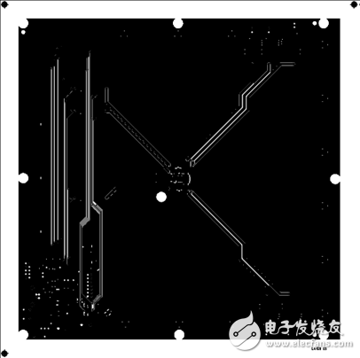
图27.评估板Si5332-12EX-EVB PCB设计图(9)
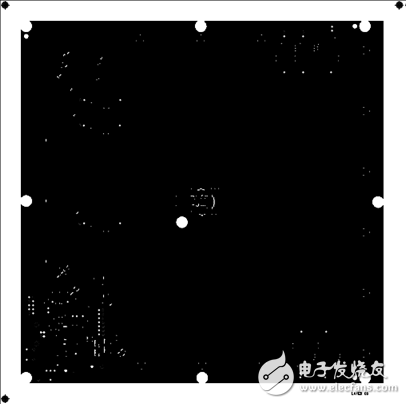
图28.评估板Si5332-12EX-EVB PCB设计图(10)
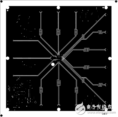
图29.评估板Si5332-12EX-EVB PCB设计图(11)
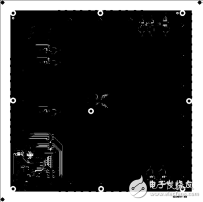
图30.评估板Si5332-12EX-EVB PCB设计图(12)
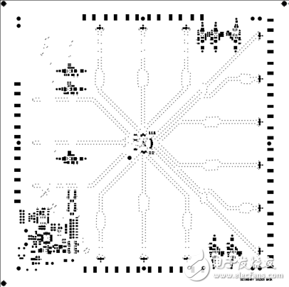
图31.评估板Si5332-12EX-EVB PCB设计图(13)

图32.评估板Si5332-12EX-EVB PCB设计图(14)
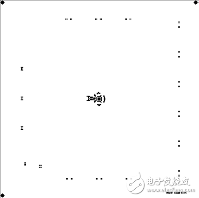
图33.评估板Si5332-12EX-EVB PCB设计图(15)

图34.评估板Si5332-12EX-EVB PCB设计图(16)
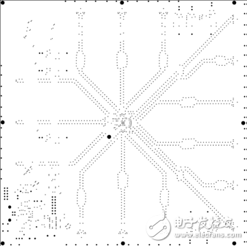
图35.评估板Si5332-12EX-EVB PCB设计图(17)
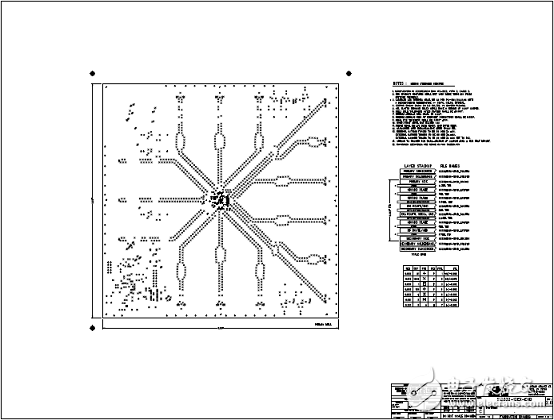
图36.评估板Si5332-12EX-EVB PCB设计图(18)
- 相关推荐
- 热点推荐
- 时钟发生器
-
Si7013EVB-UDP Si7013温湿度传感器评估套件2020-04-21 1451
-
采用Si598任意频率I2C可编程XO/VCXO的Si57X-EVB评估板2019-05-10 1672
-
评估Si5346任意频率,任意输出,抖动衰减时钟倍频器的SI5346-EVB评估板2019-02-28 2971
-
评估Si5347四路任意频率抖动衰减时钟倍频器的评估板SI5347-EVB2019-02-27 2973
-
基于Si5345任意频率,任意输出,抖动衰减时钟倍频器的评估板SI5345-EVB2019-02-26 5114
-
基于Si5344时钟倍频器的评估板SI5344-D-EVB2019-02-25 2664
-
SI5324-EVB评估板使用SI5324,0.002至710 MHz时钟发生器2019-02-22 2588
-
基于Si5347任意频率任意输出的评估板SI5347-D-EVB2019-01-30 4114
-
Silabs Si3406x系列以太网供电(PoE)管理解决方案2018-06-16 6440
全部0条评论

快来发表一下你的评论吧 !

