

PAC1934主要特性 PAC1934评估板ADM00805特性
汽车电子
描述
Microchip公司的PAC1934是带累加器的四路直流电源/能源监测器,具有总线电压监视器和电流检测放大器,直接输入到高分辨率ADC,数字电流进行功率计算和能量累加.监测周期从1ms到36个小时或更长.电源测量精度1%,24位累加器计数,2.7-5.5V工作电压,主要用在笔记本和平板电脑,网络设备,汽车电子,云,Linux和服务器计算和工业与Linux应用.本文介绍了PAC1934主要特性,框图,系统框图和功能框图,以及PAC1934评估板ADM00805主要特性,电路图,材料清单和PCB设计图.
The PAC1934 device is a four-channel energy monitor,with bus voltage monitor and current sense amplifiers thatfeed high-resolution ADCs. Digital circuitry performs power calculations and energy accumulation.
This enables energy monitoring with integration periodsfrom 1 ms up to 36 hours or longer. Bus voltage, senseresistor voltage and accumulated proportional power arestored in registers for retrieval by the system master orEmbedded Controller.
The sampling rate and energy integration period can becontrolled over SMBus or I2C. Active channel selection,one-shot measurements and other controls are also configurableby SMBus or I2C.
The PAC1934 uses real time calibration to minimize offsetand gain errors. No input filters are required for this device.
PAC1934主要特性:
• High-Side Current Monitor
- 100 mV full scale range for current sensevoltage,16b resolution default setting
- Selectable bidirectional current sense capability,
–100 mV to +100 mV range, 16-bittwo’s complement (signed) data format
- External sense resistor sets full scale currentrange
- Very low input current simplifies routing
• Wide Bus Voltage Range for Voltage Monitor
- 0V to 32V input common-mode voltage
- 16-bit resolution for voltage measurements,14b are used for power calculations
• Real Time Auto-Calibration of Offset and GainErrors for Voltage and Current, No User AdjustmentRequired
• 1% Power Measurement Accuracy over a WideDynamic Range
• On-Chip Accumulation of 28-bit Power Results forEnergy Measurement
- 48-bit power accumulator register for recordingaccumulated power data
- 24 bit Accumulator Count
- User programmable sampling rates of 8, 64,256 and 1024 samples per second
- 17 minutes of power data accumulation minimumat 1024 S/s
- >36 hours of power data accumulation minimumat 8 S/s
• 2.7V to 5.5V Supply Operation
- Separate VDD I/O pin for digital I/O
- 1.62-5.5V capable SMBus and digital I/O
- SMBus 3.0 and I2C Fast Mode Plus (1Mb/S)
• SMBus Address - 16 Options, set with Resistor
• No Input Filters Required
• ALERT Features that can be Enabled:
- ALERT on accumulator overflow
- ALERT on Conversion Complete
• 2.225 x 2.17 mm WLCSP Package
PAC1934应用:
• Notebook and Tablet Computing
• Networking
• Automotive
• Cloud, Linux and Server Computing
• Industrial
• Linux Applications
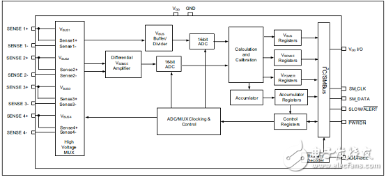
图1.PAC1934框图
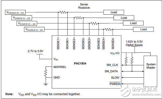
图2.PAC1934系统框图
PAC1934评估板ADM00805
The ADM00805 Evaluation Board for PAC1934 provides a flexible platform for evaluating PAC1934 and demonstrating the features of the PAC1934. A PAC1934 device ina wafer level chip scale package (WLCSP) is mounted to the board.
The ADM00805 has a USB connector to connect to a computer for device communication. The PAC1934 device may be powered directly by VBUS from the USB connectoror by an external connection for VDD.
I2C communication can be provided over USB using the on-board MCP2221 USB toI2C Bridge. There is also a header that facilitates direct I2C communication by connectingthe VDD_IO, Ground, SDA and SCL to an external source such as a PC motherboardor a Linux system.
The shorting shunts and the switch on the board facilitate either simple demonstrationof the device functions using on-board current sources or detailed evaluation offunction and performance with external sources, including prototyping the system.
The ADM00805 Evaluation Board has a PAC1934 device mounted on the board and enables direct control of all device pins and easy measurements of on-board or external voltages and currents. The I2C address is connected as 0x20 by default. Removinga shunt gives 0x22. Other addresses are possible by replacing R22 with a new value.
Sampling rate is 1024 sps by default, due to the shorting shunt on the SLOW pin connector(J23) tying the SLOW pin to ground. Remove this shunt for the SLOW sampling rate of 8 sps.
An on-board current source provides a 0.5 Hz square wave current signal for functionality testing and demo purposes. There are also on-board current sense resistors, provisions for external sources and loads, and provisions for both USB control and directI2C connection.
评估板ADM00805包括:
• The ADM00805 Evaluation Board (EVB)
• USB cable
• Important Information Sheet
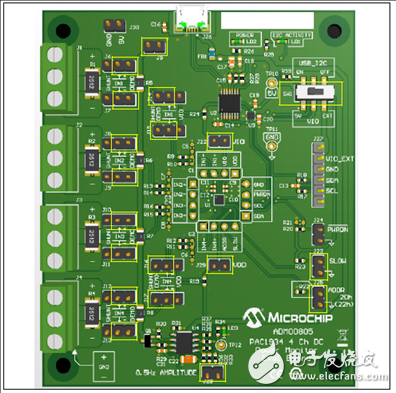
图4.评估板ADM00805外形图
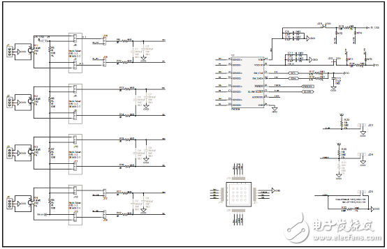
图5.评估板ADM00805电路图(1)
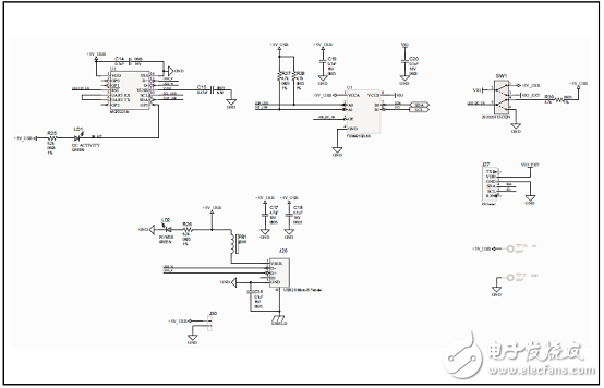
图6.评估板ADM00805电路图(2)
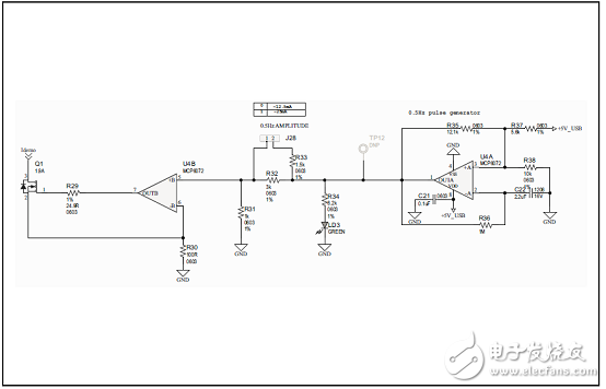
图7.评估板ADM00805电路图(3)
评估板ADM00805材料清单:
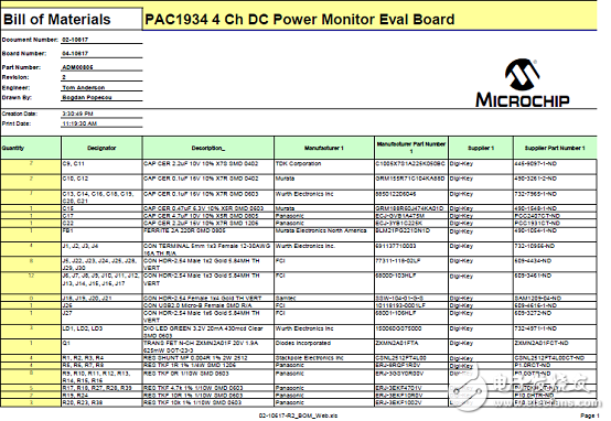
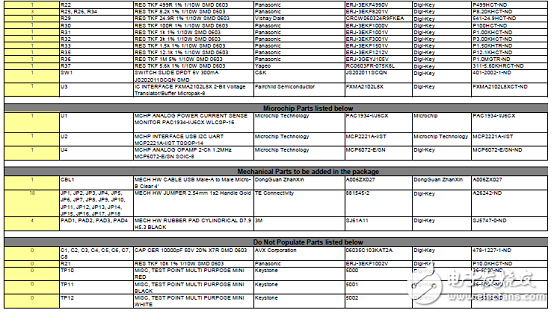
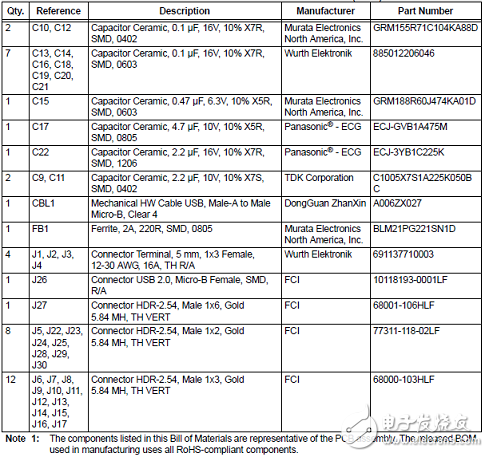
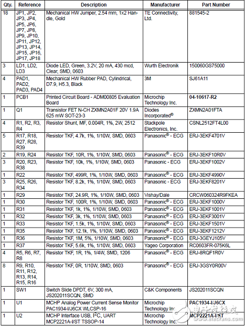
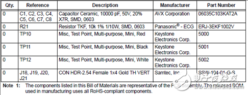
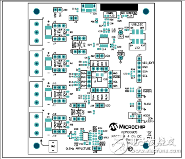
图8.评估板ADM00805 PCB设计图(1):顶层丝印
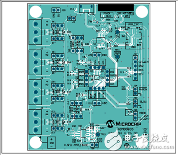
图9.评估板ADM00805 PCB设计图(2):顶层铜和丝印
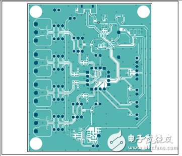
图10.评估板ADM00805 PCB设计图(3):顶层铜
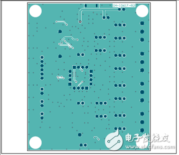
图11.评估板ADM00805 PCB设计图(4):底层铜
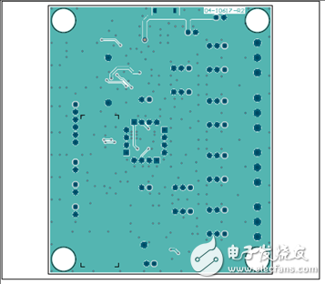
图12.评估板ADM00805 PCB设计图(5):底层铜和丝印
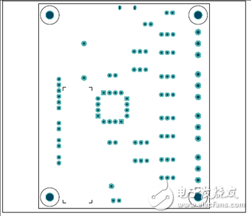
图13.评估板ADM00805 PCB设计图(6):底层丝印
详情请见:
和
以及
和
20005850B.pdf
50002673A.pdf
03-10617-R2.PDF
02-10617-R2_BOM_Web.pdf
- 相关推荐
- 热点推荐
- PAC1934
-
探索PAC - POWR1220AT8 - EV评估板:助力电源管理设计2026-05-21 104
-
AD1934:高性能8通道DAC的技术解析与应用指南2026-04-13 199
-
UM1934_基于STM32F469NI的评估板2022-11-22 552
-
DC1934A DC1934A评估板2021-08-05 290
-
PAC的基本特征有哪些?PAC有哪些功能?2021-07-02 4908
-
DC1934A-设计文件2021-05-31 460
-
PAC1934评估板用户指南2021-05-12 1026
-
DCDC转换器LT1934相关资料分享2021-04-02 1514
-
DC1934A - Design Files2021-03-10 698
-
基于PXI的PAC平台有什么应用?2019-08-14 3155
-
PAC1934 PAC1934四路高边电流传感器,具有I2C,32V,16位功率计算,累加器,双向,100mV满量程范围2019-04-18 837
-
4通道直流电源监视器PAC1934的特点及应用介绍2019-03-14 5564
-
PAC1934——4通道直流电源监视器2018-06-05 5105
-
Microchip PAC1934四路直流电源和能源监测方案2018-02-12 4651
全部0条评论

快来发表一下你的评论吧 !
