

因特尔Cyclone 10 LP FPGA评估板电路图集及PCB装配图
嵌入式软件/开发板
描述
Intel公司的Cyclone 10 LP FPGA系列是低成本和低静态功耗的器件,提供高密度可编门,板上资源和通用I/O,逻辑单元(LE)采用四输入查找表(LUT)和寄存器,嵌入乘法器区块包括一个18x18或两个9x9乘法器模式,以及用于算法加速的DSP IP,非常适合量大和低成本的智能和终端连接应用如工业和汽车电子,广播,有线和无线通信,计算和存储,医疗电子,消费类电子和智能能源,军用和航空航天.本文介绍了Cyclone 10 LP FPGA系列主要特性,LE框图,器件架构图以及Intel Cyclone 10 LP FPGA评估板主要特性,框图,电路图,材料清单和PCB装配图.
The Intel® Cyclone® 10 LP FPGAs are optimized for low cost and low static power,making them ideal for high-volume and cost-sensitive applications.
Cyclone 10 LP devices provide a high density sea of programmable gates, on-board resources, and general purpose I/Os. These resources satisfies the requirements of I/O expansion and chip-to-chip interfacing. The Cyclone 10 LP architecture suits smart and connected end applications across many market segments:
• Industrial and automotive
• Broadcast, wireline, and wireless
• Compute and storage
• Government, military, and aerospace
• Medical, consumer, and smart energy
Cyclone 10 LP FPGA系列主要特性:
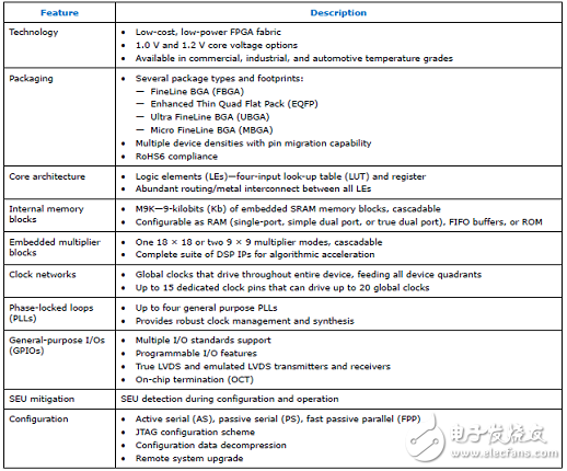
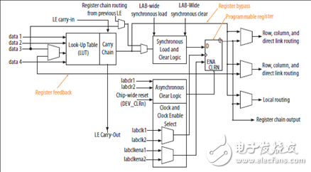
图1.Cyclone 10 LP FPGA系列LE框图
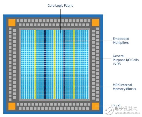
图2.Cyclone 10 LP FPGA系列架构图
The logic and routing core fabric sea of gates is surrounded on each side by I/O elements, with a phase-locked loop (PLLs) in each corner. Embedded memory blocks (M9K) and 18 x 18 bit multipliers blocks are arranged in vertical columns.
The architecture also includes highly efficient interconnect and low-skew clock networks, providing connectivity between logic structures for clock and data signals.
Cyclone 10 LP FPGA系列应用:
Intel Cyclone 10 LP FPGAs are ideal for cost-sensitive applications that require increasing lower static power as the need for scalable processing acceleration increases system interface requirements.
Typical end market examples include:
I/O expansion
Interfacing
Bridging
Sensor fusion
Industrial motor control
Intel Cyclone 10 LP FPGA评估板
The Intel® Cyclone® 10 LP Evaluation Kit provides an easy-to-use platform for evaluating the performance and features of the Intel Cyclone 10 LP FPGA device.The evaluation kit includes a RoHS and CE compliant Intel Cyclone 10 LP FPGA Evaluation Board with the following components.
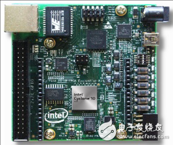
图3.Intel Cyclone 10 LP FPGA评估板外形图
Intel Cyclone 10 LP FPGA评估板特性器件:
• Intel Cyclone 10 LP FPGA (10CL025, U256 package)
• Enpirion® EN5329QI/EN5339QI - 2A/3A PowerSoC Low Profile Synchronous Buck
DC-DC Converter with Integrated Inductor
• Enpirion EP5358xUI 600 mA PowerSoC DC-DC Step-Down Converters with
Integrated Inductor
• Intel XWAY PHY11G Gigabit Ethernet PHY PEF7071
• Intel MAX® 10 FPGA 10M08SAU169C8G (Embedded Intel FPGA Download Cable II
and System Management)
Programming and Configuration
• Embedded Intel FPGA Download Cable II (JTAG)
• Optional JTAG direct via 10-pin header
• Active Serial x1 configuration from EPCQ flash
Memory Devices
• 128 Mb 8-bit HyperRAM with HBMC (Hyperbus Memory Controller) IP provided by
Synaptic Labs
• 64 Mb EPCQ Flash
Communication Ports
• One Gigabit Ethernet (GbE) RJ-45 port
• One 2x20 GPIO Expansion Header
• One Arduino UNO R3 type connectors
• One 12-pin DigilentPmod compatible connector
Clock Circuits
• Silicon Labs Si510 50 MHz crystal oscillator
• Silicon Labs Si5351 clock generator with programmable frequency GUI
Power Supply
• USB Y-cable (USB Type-A to mini Type-B) for both on-board Intel FPGA Download
Cable II and 5V power supply from USB port
• Supplemental 5V DC power adaptor option (5V power adaptor and cord are not
included in the kit)
Intel Quartus® Prime Standard Edition / Lite Edition
Intel Quartus® Prime Standard Edition / Lite Edition software can be downloaded from
the Download Center at the Intel FPGA website.
Recommended Operating Conditions
• Recommended ambient operating temperature range: 0C to 45C
• Maximum VCCINT current: 0.6 A
• Maximum board power consumption: 3 A @ 5 V when powered by AC/DC adaptor
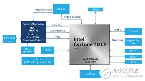
图4.Intel Cyclone 10 LP FPGA评估板框图
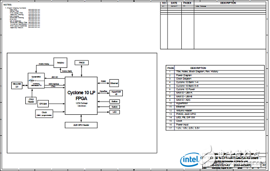
图5.Intel Cyclone 10 LP FPGA评估板电路图(1)
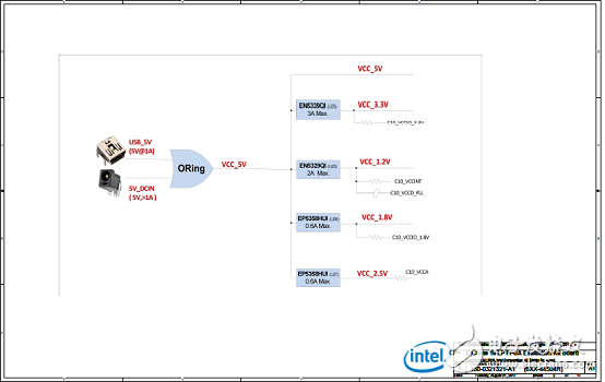
图6.Intel Cyclone 10 LP FPGA评估板电路图(2)
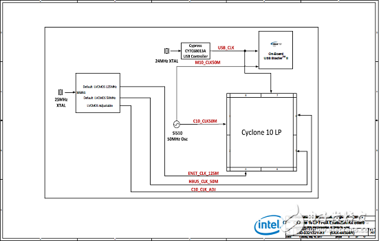
图7.Intel Cyclone 10 LP FPGA评估板电路图(3)
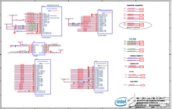
图8.Intel Cyclone 10 LP FPGA评估板电路图(4)
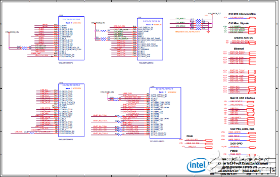
图9.Intel Cyclone 10 LP FPGA评估板电路图(5)
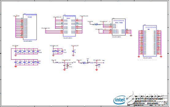
图10.Intel Cyclone 10 LP FPGA评估板电路图(6)
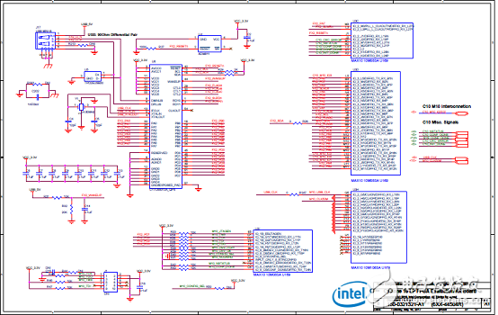
图11.Intel Cyclone 10 LP FPGA评估板电路图(7)
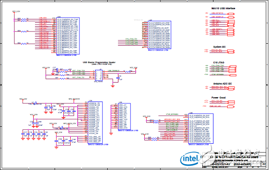
图12.Intel Cyclone 10 LP FPGA评估板电路图(8)
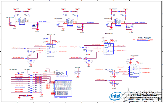
图13.Intel Cyclone 10 LP FPGA评估板电路图(9)
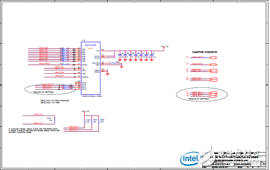
图14.Intel Cyclone 10 LP FPGA评估板电路图(10)
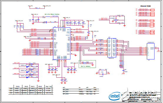
图15.Intel Cyclone 10 LP FPGA评估板电路图(11)
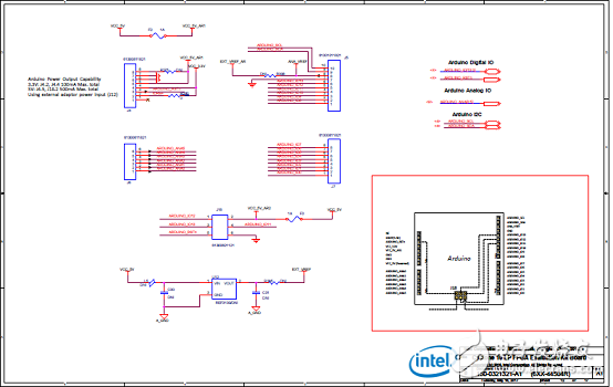
图16.Intel Cyclone 10 LP FPGA评估板电路图(12)
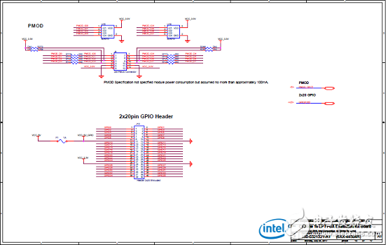
图17.Intel Cyclone 10 LP FPGA评估板电路图(13)
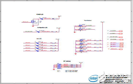
图18.Intel Cyclone 10 LP FPGA评估板电路图(14)
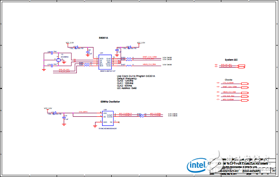
图19.Intel Cyclone 10 LP FPGA评估板电路图(15)
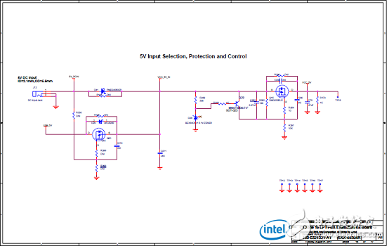
图20.Intel Cyclone 10 LP FPGA评估板电路图(16)
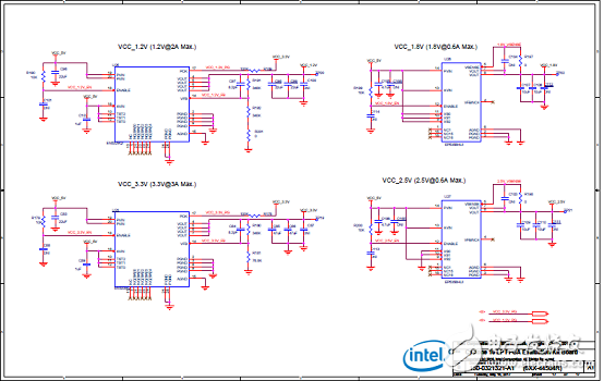
图21.Intel Cyclone 10 LP FPGA评估板电路图(17)
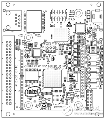
图22.Intel Cyclone 10 LP FPGA评估板PCB装配图(正面)
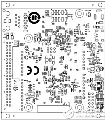
图23.Intel Cyclone 10 LP FPGA评估板PCB装配图(背面)
-
HMC1197LP7F评估PCB原理图2021-05-27 658
-
HMC821LP6CE评估PCB原理图2021-05-18 743
-
HMC1032LP6G评估。PCB原理图2021-05-14 696
-
学会装配图的识图步骤和识图要领2021-03-23 13434
-
工业机器人中的装配图要怎么画?2021-02-11 5789
-
pcb电路图有哪一些要点2020-03-31 2780
-
Altium Designer Summer 09 将PCB图输出装配图的方法2019-07-09 2978
-
STM32神舟三号装配图-TOP2015-11-10 444
-
超经典的FPGA开发指南与电路图集2015-07-16 11500
-
Cyclone1C20的Nios开发板电路图及PCB文件2012-04-19 3664
-
读懂电路图第五课--PCB布局图2010-08-22 2072
-
电动自行车电路图和充电器电路图集2009-01-21 6583
-
镗刀装配图2008-05-27 1572
-
齿轮泵结构装配图2008-05-26 9278
全部0条评论

快来发表一下你的评论吧 !

