

蓝牙低能(BLE)控制机器人设计详解
电子说
描述
NXP公司的KW40Z/30Z/20Z是超低功耗高度集成单片器件,集成了工作在2.36 GHz 到2.48 GHz支持FSK/GFSK和O-QPSK调制的无线收发器,ARM Cortex-M0+CPU,160KB闪存和20KB SRAM,BLE链接层硬件,802.15.4包处理器硬件和满足目标应用的外设.主要用在手持设备,极低功耗嵌入系统的低功耗蓝牙(BLE)或IEEE标准802.15.4 RF连接如手持保健设备,可穿戴运动和健美设备,AV遥控,计算机键盘和鼠标,游戏控制器,接入控制,安全系统,智能能源和家庭区域网.本文介绍了Kinetis KW40Z/30Z/20Z主要特性,框图,蓝牙低能(BLE)控制机器人主要特性,框图以及Kinetis KW40Z/30Z/20Z MCU开发平台FRDM-KW40Z主要特性,框图,电路图,材料清单和PCB主要设计图.
The KW40Z/30Z/20Z (called KW40Z throughout this document) is an ultra low-power,highly integrated single-chip device that enables Bluetooth low energy (BLE) or IEEEStandard 802.15.4 RF connectivity for portable, extremely low-power embedded systems. Applications include portable health care devices, wearable sports and fitness devices, AV remote controls, computer keyboards and mice, gaming controllers, access control, security systems, smart energy and home area networks.
The KW40Z SoC integrates a radio transceiver operating in the 2.36 GHz to 2.48 GHz range supporting a range of FSK/GFSK and O-QPSK modulations, an ARM Cortex-M0+CPU, 160 KB Flash and 20 KB SRAM, BLE Link Layer hardware, 802.15.4 packet processor hardware and peripherals optimized to meet the requirements of the target applications.
The KW40Z SoC’s radio frequency transceiver is compliant with Bluetooth version 4.1 for Low Energy (aka Bluetooth Smart), and the IEEE standard 802.15.4-2011 using OQPSKin the 2.4 GHz ISM band.
The KW40Z SoC can be used in applications as a "BlackBox" modem by simply adding BLE or IEEE Std. 802.15.4 connectivity to an existing embedded controller system, or used as a stand-alone smart wireless sensor with embedded application where no host controller is required.
Freescale provides fully certified protocol stacks and application profiles to support KW40Z. The KW40Z Flash and SRAM memory are available for applications and communication protocols using a choice of Freescale or 3rd party software development tools.
The RF section of the KW40Z SoC is optimized to require very few externalcomponents, achieving the smallest RF footprint possible on a printed circuit board.
Extremely long battery life is achieved though efficiency of code execution in the Cortex-M0+ CPU core and the multiple low power operating modes of the KW40Z SoC. Additionally, an integrated DC-DC converter enables a wide operating range from 0.9 V to 4.2 V. The DC-DC in Buck mode enables KW40Z to operate from a single coin cell battery with a significant reduction of peak Rx and Tx current consumption. The DC-DC in boost mode enables a single alkaline battery to be used throughout its entire useful voltage range of 0.9 V to 1.795 V.
Kinetis KW40Z主要特性:
• Multi-Standard Radio
– 2.4 GHz Bluetooth Low Energy version 4.1compliant
– IEEE Standard 802.15.4 2011 compliant
– Typical Receiver Sensitivity (BLE) = -91 dBm
– Typical Receiver Sensitivity (802.15.4) = -102 dBm
– Programmable Transmitter Output Power: -18 dBmto +5 dBm
– Low external component counts for low costapplication
• MCU and Memories
– Up to 48 MHz ARM® Cortex-M0+ core
– On-chip 160 KB Flash memory
– On-chip 20 KB SRAM
• Low Power Consumption
– Typical Rx Current: 6.5 mA (DCDC in buck mode,3.6 V supply)
– Typical Tx Current: 8.4 mA (DCDC in buck mode,3.6 V supply) for a 0 dBm output
– Low Power Mode (VLLS0) Current: 206 nA
• Clocks
– 32 MHz Crystal Oscillator
– 32 kHz Crystal Oscillator
• System peripherals
– Nine low-power modes to provide poweroptimization based on application requirements
– DCDC Converter supporting Buck, Boost, andBypass modes
– DMA Controller
– COP Software watchdog
– SWD Interface and Micro Trace buffer
– Bit Manipulation Engine (BME)
• Human-machine interface
– Touch Sensing Input
– General-purpose input/output
• Analog modules
– 16-bit Analog-to-Digital Converter (ADC)
– 12-bit Digital-to-Analog Converter (DAC)
– 6-bit High Speed Analog Comparator (CMP)
• Timers
– 16-bit low-power timer (LPTMR)
– 3 Timers Modules(TPM): One 4 channels TPM andTwo 2 channels TPMs
– Programmable Interrupt Timer (PIT)
– Real-Time Clock (RTC)
• Communication interfaces
– 2 SPI modules
– 2 I2C modules
– Low Power UART module
– Carrier Modulator Timer (CMT)
• Security
– AES-128 Accelerator (AESA)
– True Random Number Generator (TRNG)
• Operating Characteristics
– DCDC Converter supporting Buck, Boost, andBypass modes
– Temperature range (ambient): -40 to 85℃
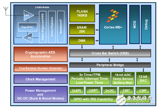
图1.Kinetis KW40Z/302/202简化框图
无线电特性:
Operating frequencies:
• 2.4 GHz ISM band (2400-2483.5 MHz)
• MBAN 2360-2400 MHz
Supported standards:
• Bluetooth v4.1 Low Energy compliant 1 Mbps GFSK modulation
• IEEE Std. 802.15.4-2011 compliant O-QPSK modulation
• Freescale Thread Networking Stack
• Bluetooth Low Energy(BLE) Application Profiles
• ZigBee PRO and application profiles
Receiver performance:
• Receive sensitivity of -91 dBm for BLE
• Receive sensitivity of -102 dBm typical for IEEE Std. 802.15.4
Other features:
• Programmable transmit output power from -18 dBm to +5 dBm with DC/DC bypassand buck modes of operation
• Bluetooth Low Energy Link Layer hardware
• Hardware acceleration for IEEE Std. 802.15.4 packet processing
• 32 MHz crystal reference oscillator
• Supports antenna diversity option for IEEE Std. 802.15.4
• Supports dual PAN for IEEE Std. 802.15.4 with hardware-assisted address matching
acceleration
• Differential RF port shared by transmit and receive
• Low external component count
• Supports transceiver range extension using external PA and/or LNA
MCU特性:
ARM Cortex-M0+ CPU
• Up to 48 MHz CPU
• As compared to Cortex-M0, the Cortex-M0+ uses an optimized 2-stage pipeline
microarchitecture for reduced power consumption and improved architecturalperformance (cycles per instruction)
• Supports up to 32 interrupt request sources
• Binary compatible instruction set architecture with the Cortex-M0 core
• Thumb instruction set combines high code density with 32-bit performance
• Serial Wire Debug (SWD) reduces the number of pins required for debugging
• Micro Trace Buffer (MTB) provides lightweight program trace capabilities usingsystem RAM as the destination memory
Nested Vectored Interrupt Controller (NVIC)
• 32 vectored interrupts, 4 programmable priority levels
• Includes a single non-maskable interrupt
Wake-up Interrupt Controller (WIC)
• Supports interrupt handling when system clocking is disabled in low power modes
• Takes over and emulates the NVIC behavior when correctly primed by the NVIC onentry to very-deep-sleep
• A rudimentary interrupt masking system with no prioritization logic signals forwake-up as soon as a non-masked interrupt is detected
Debug Controller
• Two-wire Serial Wire Debug (SWD) interface
• Hardware breakpoint unit for 2 code addresses
• Hardware watchpoint unit for 2 data items
• Micro Trace Buffer for program tracing
On-Chip Memory
• 160 KB Flash
• Firmware distribution protection. Flash can be marked execute-only on a persector(4 KB) basis to prevent firmware contents from being read by 3rd parties
• Flash implemented as one 128 KB block and one 32 KB block. Code canexecute or read from one block while the other block is being erased orprogrammed
• 20 KB SRAM
• Security circuitry to prevent unauthorized access to RAM and flash contents throughthe debugger
系统特性:
Power Management Control Unit (PMC)
• Programmable power saving modes
• Available wake-up from power saving modes via internal and external sources
• Integrated Power-on Reset (POR)
• Integrated Low Voltage Detect (LVD) with reset (brownout) capability
• Selectable LVD trip points
• Programmable Low Voltage Warning (LVW) interrupt capability
• Individual peripheral clocks can be gated off to reduce current consumption
• Internal Buffered bandgap reference voltage
• Factory programmed trim for bandgap and LVD
• 1 kHz Low Power Oscillator (LPO)
DC-DC Converter
• Internal switch mode power supply supporting Buck, Boost, and Bypass operating
Modes
• Buck operation supports external voltage sources of 2.1 V to 4.2 V. This reduces
peak current consumption during Rx and Tx by ~25%, ideal for single coin-cellbattery operation (typical CR2032 cell).
• Boost operation supports external voltage sources of 0.9V to 1.795V, which isefficiently increased to the static internal core voltage level, ideal for single batteryoperation (typical AA or AAA alkaline cell).
• When DCDC is not used, the device supports an external voltage range of 1.45V to3.6V (1.45 - 3.6V on VDD_RF1, VDD_RF2, VDD_XTAL andVDD_1P45OUT_PMCIN pins. 1.71 - 3.6V on VDD_0, VDD_1 and VDDA pins)
• An external inductor is required to support the Buck or Boost modes
• The DCDC Converter 1.8V output current drive for external devices (MCU in RUN
mode, Radio is enabled, other peripherals are disabled)
• Up to 44mA in buck mode with VDD_1P8 = 1.8V
• Up to 31.4mA in buck mode with VDD_1P8 = 3.0V
DMA Controller
• Four independently programmable DMA controller channels provides the means todirectly transfer data between system memory and I/O peripherals
• DMA controller is capable of functioning in run and wait modes of operation
• Dual-address transfers via 32-bit master connection to the system bus
• Data transfers in 8-, 16-, or 32-bit blocks
• Continuous-mode or cycle-steal transfers from software or peripheral initiation
DMA Channel Multiplexer (DMA MUX)
• 4 independently selectable DMA channel routers
• 2 periodic trigger sources available
• Each channel router can be assigned to 1 of the peripheral DMA sources
COP Watchdog Module
• Independent clock source input (independent from CPU/bus clock)
• Choice between two clock sources
• LPO oscillator
• Bus clock
System Clocks
• 32 MHz crystal reference oscillator provides clock for the radio, and is the mainclock option for the MCU
• 32/32.768 kHz crystal reference oscillator used to maintain precise Bluetooth radiotime in low power modes
• Multipurpose Clock Generator (MCG)
• Internal reference clocks — Can be used as a clock source for other on-chipperipherals
• On-chip RC oscillator range of 31.25 kHz to 39.0625 kHz with 2% accuracyacross full temperature range
• On-chip 4MHz oscillator with 5% accuracy across full temperature range
• Frequency-locked loop (FLL) controlled by internal or external reference
• 20 MHz to 48 MHz FLL output
Unique Identifiers
• 10 bytes of the Unique ID represents a unique identifier for each chip
• 40 bits of unique MAC address can be used to generate BLE or 802.15.4 deviceAddress
外设特性:
16-bit Analog-to-Digital Converter (ADC)
• Linear successive approximation algorithm with 16-bit resolution
• Output formatted in 16-, 12-, 10-, or 8-bit right justified format
• Single or continuous conversion
• Configurable sample time and conversion speed / power
• Conversion rates in 16-bit mode with no averaging up to ~500Ksamples/sec
• Input clock selection
• Operation in low power modes for lower noise operation
• Asynchronous clock source for lower noise operation
• Selectable asynchronous hardware conversion trigger
• Automatic compare with interrupt for less-than, or greater than, or equal toprogrammable value
• Temperature sensor
• Battery voltage measurement
• Hardware average function
• Selectable voltage reverence
• Self-calibration mode
12-Bit Digital-to-Analog Converter (DAC)
• 12-bit resolution
• Guaranteed 6-sigma monotonicity over input word
• High- and low-speed conversions
• 1 μs conversion rate for high speed, 2 μs for low speed
• Power-down mode
Feature Descriptions
• Automatic mode allows the DAC to generate its own output waveforms includingsquare, triangle, and sawtooth
• Automatic mode allows programmable period, update rate, and range
• DMA support with configurable watermark level
High-Speed Analog Comparator (CMP)
• 6-bit DAC programmable reference generator output
• Up to eight selectable comparator inputs; each input can be compared with any input
by any polarity sequence
• Selectable interrupt on rising edge, falling edge, or either rising or falling edges ofcomparator output
• Two performance modes:
• Shorter propagation delay at the expense of higher power
• Low power, with longer propagation delay
• Operational in all MCU power modes
Low Power Timer (LPTMR)
• One channel
• Operation as timer or pulse counter
• Selectable clock for prescaler/glitch filter
• 1 kHz internal LPO
• External low power crystal oscillator
• Internal reference clock
• Configurable glitch filter or prescaler
• Interrupt generated on timer compare
• Hardware trigger generated on timer compare
• Functional in all power modes
Timer/PWM (TPM)
• TPM0: 4 channels, TPM1 and TPM2: 2 channels each
• Selectable source clock
• Programmable prescaler
• 16-bit counter supporting free-running or initial/final value, and counting is up or updown
• Input capture, output compare, and edge-aligned and center-aligned PWM modes
• Input capture and output compare modes
• Generation of hardware triggers
• TPM1 and TPM2: Quadrature decoder with input filters
• Global time base mode shares single time base across multiple TPM instances
Programmable Interrupt Timer (PIT)
• Up to 2 interrupt timers for triggering ADC conversions
• 32-bit counter resolution
• Clocked by system clock frequency
Real-Time Clock (RTC)
• 32-bit seconds counter with 32-bit alarm
• Can be invalidated on detection of tamper detect
• 16-bit prescaler with compensation
• Register write protection
• Hard Lock requires MCU POR to enable write access
• Soft lock requires system reset to enable write/read access
• Capable of waking up the system from low power modes
Inter-Integrated Circuit (I2C)
• Two channels
• Compatible with I2C bus standard and SMBus Specification Version 2 features
• Up to 1 Mbps operation
• Multi-master operation
• Software programmable for one of 64 different serial clock frequencies
• Programmable slave address and glitch input filter
• Interrupt driven byte-by-byte data transfer
• Arbitration lost interrupt with automatic mode switching from master to slave
• Calling address identification interrupt
• Bus busy detection broadcast and 10-bit address extension
• Address matching causes wake-up when processor is in low power mode
LPUART
• One channel
• Full-duplex operation
• Standard mark/space non-return-to-zero (NRZ) format
• 13-bit baud rate selection with fractional divide of 32
• Programmable 8-bit or 9-bit data format
• Programmable 1 or 2 stop bits
• Separately enabled transmitter and receiver
• Programmable transmitter output polarity
• Programmable receive input polarity
• 13-bit break character option
• 11-bit break character detection option
• Two receiver wakeup methods:
• Idle line wakeup
• Address mark wakeup
• Address match feature in receiver to reduce address mark wakeup ISR overhead
• Interrupt or DMA driven operation
• Receiver framing error detection
• Hardware parity generation and checking
• Configurable oversampling ratio to support from 1/4 to 1/32 bit-time noise detection
• Operation in low power modes
• Hardware Flow Control RTSCTS
• Functional in Stop/VLPS modes
Serial Peripheral Interface (DSPI)
• Two independent SPI channels
• Master and slave mode
• Full-duplex, three-wire synchronous transfers
• Programmable transmit bit rate
• Double-buffered transmit and receive data registers
• Serial clock phase and polarity options
• Slave select output
• Control of SPI operation during wait mode
• Selectable MSB-first or LSB-first shifting
• Support for both transmit and receive by DMA
Carrier Modulator Timer (CMT)
• Four modes of operation
• Time; with independent control of high and low times
• Baseband
• Frequency shift key (FSK)
• Direct software control of CMT_IRO signal
• Extended space operation in time, baseband, and FSK modes
• Selectable input clock divider
• Interrupt on end of cycle
• Ability to disable CMT_IRO signal and use as timer interrupt
General Purpose Input/Output (GPIO)
• Hysteresis and configurable pull up device on all input pins
• Independent pin value register to read logic level on digital pin
• All GPIO pins can generate IRQ and wakeup events
• Configurable drive strength on some output pins
Touch Sensor Input (TSI)
• Support up to 16 external electrodes
• Automatic detection of electrode capacitance across all operational power modes
• Internal reference oscillator for high-accuracy measurement
• Configurable software or hardware scan trigger
• Fully support Freescale touch sensing software (TSS) library
• Capability to wake MCU from low power modes
• Compensate for temperature and supply voltage variations
• High sensitivity change with 16-bit resolution register
• Configurable up to 4096 scan times
• Support DMA data transfer
Keyboard Interface
• GPIO can be configured to function as a interrupt driven keyboard scanning matrix
• In the 48pin package there are a total of 28 digital pins
• In the 32pin package there are a total of 15 digital pins
• These pins can be configured as needed by the application as GPIO, UART, SPI,
I2C, ADC, timer I/O as well as other functions
AES Accelerator (AESA)
• The Advanced Encryption Standard Accelerator (AESA) is a stand-alone symmetric
encryption accelerator supporting 128- bit key and data size and the followingmodes:
• Electronic Codebook (ECB)
• Cipher Block Chaining (CBC)
• Counter (CTR)
• CTR & CBC-MAC (CCM and CCM*)
• Cipher-base MAC (CMAC)
• Extended Cipher Block Chaining Message Authentication Code (XCBC-MAC)
• The AESA supports all BLE and IEEE 802.15.4 packet sizes
• The AESA supports DMA and interrupt-driven operation
True Random Number Generator (TRNG)
• The TRNG is an entropy source
• The TRNG output is intended to be read and used as an input to a deterministicrandom number generator
• The deterministic random number general will be implemented in software
• A FIPS 180 compliant solution can be realized using the TRNG together with a FIPS
compliantdeterminstic random number generator and SoC-level security
蓝牙低能(BLE)控制机器人参考设计
The Bluetooth® Low Energy (BLE) controlled robot reference deign is developed using FRDM-KW40 board and PololuZumo Robot and can be controlled using a cellphone app. The BLE controlled robot is powered by the Kinetis KW40Z system on chip (SoC), which includes an ARM® Cortex® M0+ processor together with a 2.4 GHz radio for BLE and 802.15.4. It is implemented using the HID over GATT profile and works as a human interface device. The software is designed with features such as BLE data transfer to cellphone app, motor control and battery monitoring.
图2.蓝牙低能(BLE)控制机器人外形图
蓝牙低能(BLE)控制机器人主要特性:
Includes the NXP ultra-low-power Kinetis KW40Z SoC that enables Bluetooth® Smart/Bluetooth® Low Energy (BLE) v4.1 and/or IEEE® 802.15.4-2011 RF connectivity for portable, extremely low-power embedded systems
Developed using Kinetis Software Development Kit (SDK), comprehensive software support for Kinetis MCUs and includes a hardware abstraction layer (HAL) and drivers for each MCU peripheral, connectivity stacks, middleware, real-time operating systems and example applications designed to simplify and accelerate application development on Kinetis MCUs
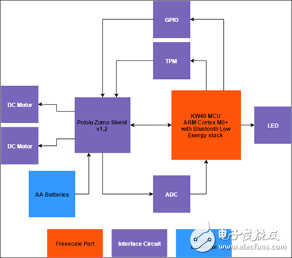
图3.蓝牙低能(BLE)控制机器人框图
Kinetis KW40Z/30Z/20Z MCU开发平台FRDM-KW40Z
The ZumoBot Reference Design is initially provided with the ZumoBot mobile application. This application interacts with the ZumoBot. It enables scanning BLE devices, service discovery, battery measurement, and ZumoBot control using the HID profile. This document targets on the Freescale Freedom FRDM-KW40Z development board. This section details the hardware and software requirements to use the ZumoBot.
The ZumoBot firmware application is designed to run on the Freescale FRDM-KW40Z board.
The FRDM-KW40Z is a low-cost development platform enabled by the Kinetis W series KW40Z/30Z/20Z (KW40Z) family built on the ARM® Cortex®-M0+ processor featuring an integrated 2.4 GHz transceiver supporting Bluetooth® Smart/Bluetooth®Low Energy (BLE) v4.1 and/or IEEE® 802.15.4-2011 standards.
The FRDM-KW40Z kit contains two boards, enabling point-to-point out of the box connectivity. Each board can be configured as a Freedom development board or as a Freedom shield. The FRDM-KW40Z hardware is form-factor compatible with the Arduino™ R3 pin layout, providing a broad range of expansion board options.
The FRDM-KW40Z features a highly-sensitive, optimized 2.4 GHz radio with PCB F-antenna which can be bypassed for connection to test equipment via SMA connection, multiple power supply options, push and capacitive touch buttons, switches, LEDs and integrated sensors.
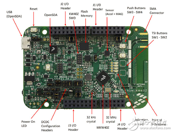
图4.MCU开发平台FRDM-KW40Z外形图
MCU开发平台FRDM-KW40Z主要特性:
Supports MKW40Z160VHT4, MKW30Z160VHM4, MKW20Z160VHT4 Kinetis W MCUs Radio (RF) Features
High-performance 2.4 GHz transceiver supporting Bluetooth Low Energy (BLE) v4.1 and IEEE 802.15.4-2011
-91 dBm BLE and -102 dBm 802.15.4 receive sensitivity
Up to +5 dBm programmable transmit output power
6.5 mA / 8.4 mA Rx/Tx power consumption (DC/DC enabled)
PCB inverted F-type antenna and SMA RF port
Minimum number of matching components and external balun
External 256 KB Serial Flash supporting Over-the-air firmware updates
MCU Features
Up to 48 MHz Cortex-M0+ MCU
160 KB Flash, 20 KB SRAM
DMA, ADC, DAC, CMP, TMRs, SPI, I2C, UART, CMT
AES128 Security Hardware and True Random Number Generator
Multiple DCDC power supply options (Bypass, Buck, Boost)
Software/Protocol Stacks
Bluetooth Low Energy Host Stack and Application Profiles
Thread (end device only)
ZigBee Pro and Application Profiles
IEEE 802.15.4-2011 MAC/PHY
NXP Simple MAC (SMAC)
Multiple switches, push and capacitive tough buttons, LEDs, infrared
FXOS8700CQ - low-power 6-axis linear accelerometer and magnetometer
OpenSDA debug interface
Arduino compatible
Kit Contains
2 FRDM-KW40Z Freedom Development Boards
Quick Reference Card
2 USB Cables
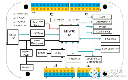
图5.MCU开发平台FRDM-KW40Z功能框图
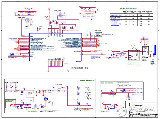
图6.MCU开发平台FRDM-KW40Z电路图(1)
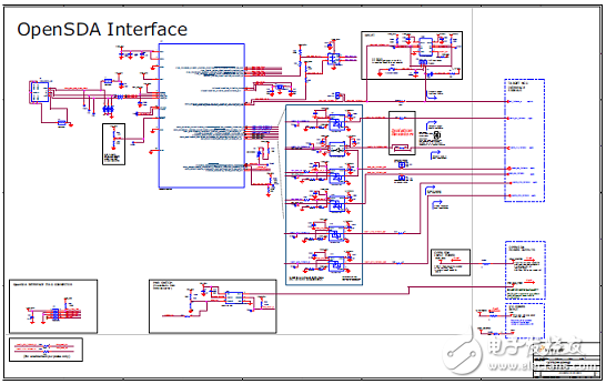
图7.MCU开发平台FRDM-KW40Z电路图(2)
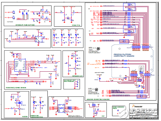
图8.MCU开发平台FRDM-KW40Z电路图(3)
MCU开发平台FRDM-KW40Z材料清单:
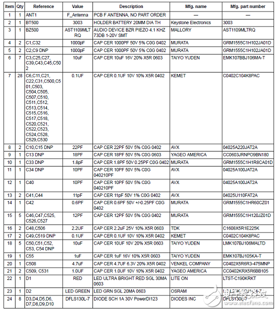
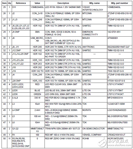
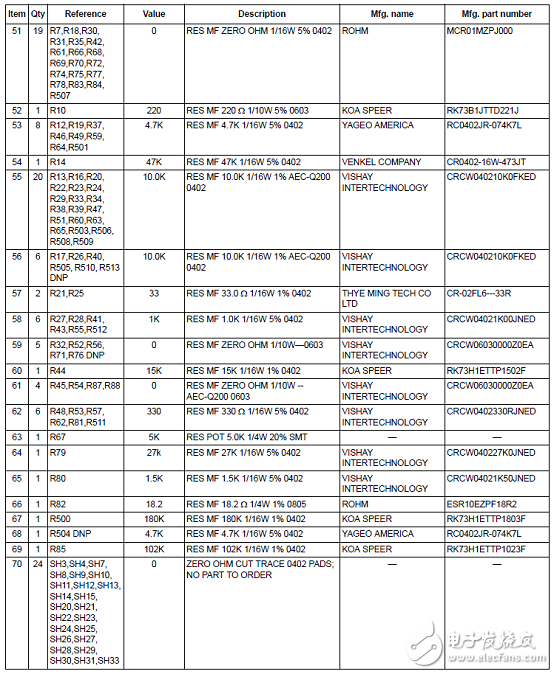
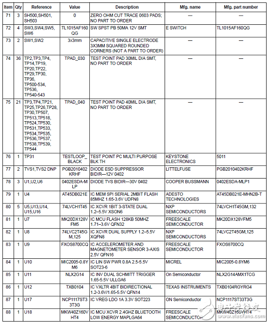

图9.MCU开发平台FRDM-KW40Z PCB元件布局图(顶层)
图10.MCU开发平台FRDM-KW40Z PCB元件布局图(底层)
图11.MCU开发平台FRDM-KW40Z PCB设计图(顶层)
图12.MCU开发平台FRDM-KW40Z PCB设计图(底层)
-
如何去实现一种气动爬行机器人设计2022-01-13 1644
-
刚柔软机器人设计与仿真分析实例解析2021-09-02 4501
-
机器人设计中PID控制的编程方法是什么?2021-06-30 1837
-
机器人设计教程之机器人控制和决策子系统2018-12-25 1951
-
蓝牙低能耗(BLE)的其他技术特点2018-11-22 5261
-
《机器人设计与实现》——低成本DIY机器人,一本机器人制作的经典入门书2017-08-01 194179
-
智能搬运机器人设计2017-01-22 1165
-
机器人设计方案,控制系统设计汇总2014-06-30 2966
-
智能机器人设计资料大全2014-06-04 166331
-
蓝牙控制机器人端2013-07-20 4768
-
红外遥控六足爬虫机器人设计2013-02-19 4670
-
基于视觉的高速寻线机器人设计与实现2012-09-08 2927
-
[分享]LabVIEW 与机器人设计2009-05-30 9122
全部0条评论

快来发表一下你的评论吧 !

