

基于Arria 10 SoC FPGA的高性能低成本解决方案
电子说
描述
Intel公司的Arria 10 SoC FPGA采用TSMC 20nm工艺技术,集成了双核ARM Cortex-A9MPCore硬件处理器系统(HPS)和业界一流可编逻辑技术诸如硬件浮点数字信号处理器(DSP)区块,提供具有丰富特性的嵌入外设,硬化浮点可变精度DSP区块,嵌入高速收发器,硬存储器控制器和协议IP控制器,CPU工作频率高达1.5GHz,主要用在无线基础设备,计算和存储设备,广播设备,军用设备和智能设备,有线100G线路卡,40G GPON,测试测量设备以及医疗图像诊断设备。本文介绍了Arria 10 SoC FPGA主要特性,框图以及Arria 10 SoC开发板主要特性,电源分布网络图和电路图。
The 20 nm ARM*-based Intel® Arria® 10 SoC delivers optimal performance, power efficiency, small form factor, and low cost for midrange applications. The Intel Arria 10 SoC, based on TSMC’s 20 nm process technology, combines a dual-core ARM Cortex*-A9 MPCore* Hard Processor System (HPS) with industry-leading programmable logic technology that includes hardened floating-point digital signal processing (DSP) blocks. The Intel Arria 10 SoC offers a processor with a rich feature set of embedded peripherals, hardened floating-point variable-precision DSP blocks, embedded high-speed transceivers, hard memory controllers, and protocol intellectual property (IP) controllers - all in a single highly integrated package.Intel Arria 10 SoCs: Higher System-Level Integration SoC in Production.
The Intel Arria 10 SoC combines architectural innovations with TSMC’s 20 nm process technology to deliver improvements in performance and power reduction:
65% higher processor performance with up to 1.5 GHz CPU operation per core
60% higher performance versus the previous generation, over 500 MHz-capable FPGA logic core performance (15% higher performance than previous SoC)
4X more transceiver bandwidth versus the previous generation (2X more bandwidth versus previous high-end FPGAs)
4X higher system performance (2,400 Mbps DDR4 SDRAM, Hybrid Memory Cube support)
More than 1,500 giga floating-point operation per second (GFLOPs) and up to 50 GFLOPs per Watt in a single device40% lower power with process technology improvement and innovative techniques for power reductionDesigned for Productivity
Design productivity is one of the driving philosophies of the Intel Arria 10 SoC architecture. The Intel Arria 10 SoC offers full software compatibility with previous generation SoC FPGAs, a broad ecosystem of ARM software and tools, and the enhanced FPGA and DSP hardware design flow.
Extensive ecosystem of ARM for software development.
Intel SoC FPGA Embedded Design Suite (SoC EDS) featuring the ARM* Development Studio 5* (DS-5*) Intel SoC FPGA Edition
Board support packages are available for popular operating system including Linux*, Wind River VxWorks, Wind River Linux, MicriumuC/OS-II and uC/OS-III, and more
Full software compatibility between 28 nm Cyclone® V SoC, Arria V SoC, and Intel Arria 10 SoC
Intel Quartus® Prime software FPGA design suite featuring:
High-level automated design flow with Open Computing Language (OpenCL™) compiler
Model-based digital signal processing (DSP) hardware design with DSP Builder for Intel FPGA
The Intel Arria 10 SoCs have been designed to meet the performance, power, and cost requirements for applications such as:
Wireless infrastructure equipment including remote radio unit and mobile backhaul
Compute and storage equipment including flash cache, cloud computing, and acceleration
Broadcast studio and distribution equipment including professional A/V and video conferencing
Military guidance, control, and intelligence equipment
Wireline 100G line cards, bridges and aggregation, 40G GPON
Test and measurement equipment
Diagnostic medical imaging equipment
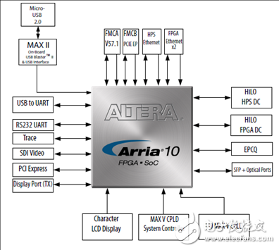
图1. Intel® Arria® 10 SoC框图
Arria 10 SoC开发板
The Arria 10 SoC development board provides a hardware platform for developing and prototyping lowpower,high-performance, and logic-intensive designs using Altera’s? Arria 10 SoC. The board provides awide range of peripherals and memory interfaces to facilitate the development of Arria 10 SoC designs.
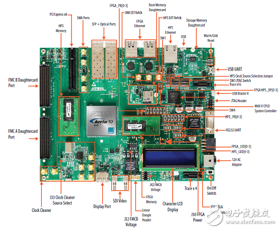
图2.Arria 10 SoC开发板外形图
Arria 10 SoC开发板主要特性:
• Arria 10 Soc (10AS066N3F40E2SG) in a 1517-pin FBGA (FineLine Ball-Grid Array) package
• FPGA configuration circuitry
• Active Serial (AS) x1 or x4 configuration (EPCQ1024L)
• MAX? V CPLD (5M2210ZF256) in a 256-pin FBGA package as the system controller
• MAX V CPLD (5M2210ZF256) in a 256-pin FBGA package as the I/O multiplier CPLD
• Clocking circuitry
• SI5338 programmable oscillator
• LMK04828 clock cleaner
• HPS clock options: 25 MHz, 33 MHz, and SMA input (2V5 LVCMOS)
• SI5112 100MHz clock generator for PCIe interface
• SI516 148.5 MHz voltage control oscillator for SDI interface
• Supported Memory
• HPS memory size (HILO card):
• 2GB DDR3 (256Mb x 40 x dual rank)
• 1GB DDR3 (256Mb x 40 x single rank)
• 1GB DDR4 (256Mb x 40 x single rank) - ships with kit
• FPGA memory size (HILO Card):
• 4GB DDR3 (256Mb x72 x dual rank)
• 2GB DDR3 (256Mb x72 x single rank)
• 2GB DDR4 (256Mb x 72 x single rank) - ships with kit
• 16MB QDRV (4Mb x 36)
• 128MB RLDRAM3(16Mb x 72)
• HPS Boot Flash (Flash card):
• NAND flash (x8) : 128MB (MT29F1G08ABBEAH4) - ships with kit
• QSPI flash: 128MB (MT25QU01GBBA8E12-0SIT) - ships with kit
• SD Micro flash card: 4GB (Kingston) - ships with kit
• Optional FPGA File Flash (Flash card):
• NAND flash (x8): 128MB (MT29F1G08ABBEAH4)
• QSPI flash: 128MB (MT25QU01GBBA8E12-0SIT)
• SD Micro flash card: 4GB (Kingston)
• Communication ports
• HPS Communication ports:
• USB 2.0 port (PHY PN: USB3320C-EZK)
• RGMII 10/100/1000 Ethernet port (PHY PN: KSZ9031RNXCA)
• USB-UART port (FT232R)
• DB-9 RS-232 Port (MAX3221)
• I2C port (I2C1 of shared I/O bit 12 and 13)
• FPGA I/O connections:
• FPGA V57.1 High Pin Count FMC slot
• FPGA Altera Low Pin Count FMC slot
• FMC_PCIe Gen2 x8 EP cable
• FPGA PCIe GEN1/2/3 x8 RC slot
• FPGA Communication ports:
• 2x SGMII Gigabit Ethernet ports (PHY PN: 88E1111-B2-NDC2C000)
• 2x 10Gb/s SFP+ ports
• Display port (DP)
• SDI/SDO video port
• SPI port
• UART port
• FPGA Debug ports:
• 16-bit Trace port (FPGA Trace)
• General user I/O
• LEDs and displays
• 4x FPGA user LEDs
• 4x HPS user LEDs
• Configuration load LED
• Configuration done LED
• Error LED
• 3x Configuration select LEDs
• 4x On-board USB-Blaster II status LEDs
• 2x FMC interface LEDs
• 2x UART data transmit and receive LEDs
• Power on LED
• Two-line character LCD display
• Push buttons
• CPU cold reset push button and one CPU warm reset push button
• Logic reset push button
• Program select push button
• Program configuration push button
• 4x FPGA user push buttons
• 4x HPS user push buttons
• External interrupt push button
• DIP Switches
• JTAG chain control DIP switch
• Board settings DIP switch
• FPGA configuration mode DIP switch
• General user DIP switch
• Power supply
• 12V DC Input
• Mechanical
• 7.175“ x 9.3” rectangular form factor
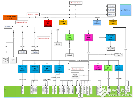
图3.Arria 10 SoC开发板电源分布网络图
图4.Arria 10 SoC开发板电路图(1)
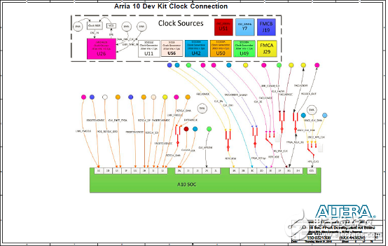
图5.Arria 10 SoC开发板电路图(2)
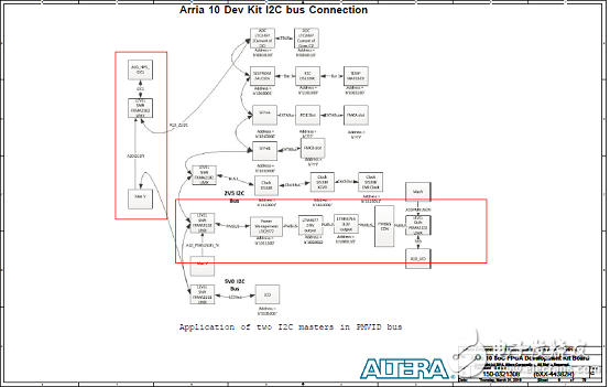
图6.Arria 10 SoC开发板电路图(3)
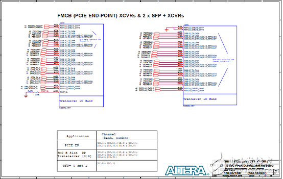
图7.Arria 10 SoC开发板电路图(4)
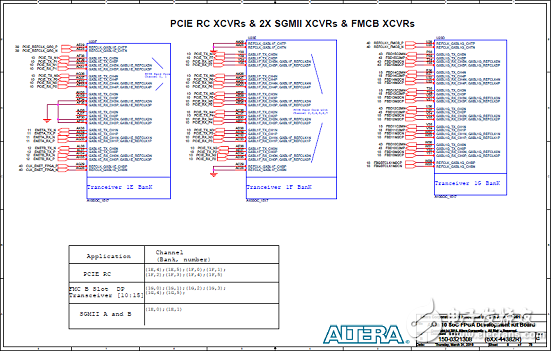
图8.Arria 10 SoC开发板电路图(5)
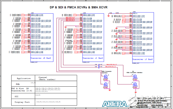
图9.Arria 10 SoC开发板电路图(6)
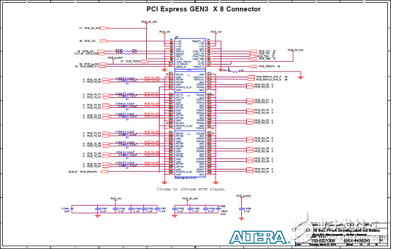
图10.Arria 10 SoC开发板电路图(7)
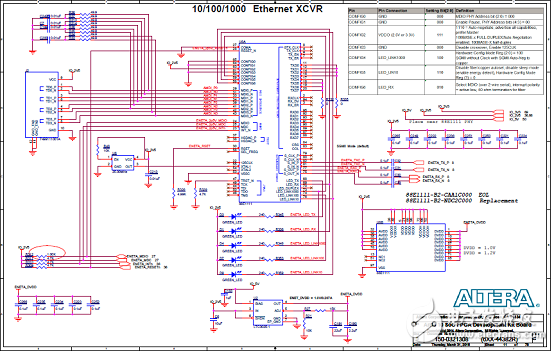
图11.Arria 10 SoC开发板电路图(8)
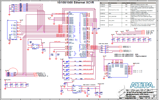
图12.Arria 10 SoC开发板电路图(9)

图13.Arria 10 SoC开发板电路图(10)
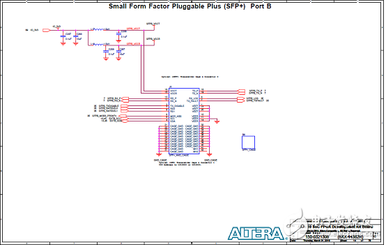
图14.Arria 10 SoC开发板电路图(11)
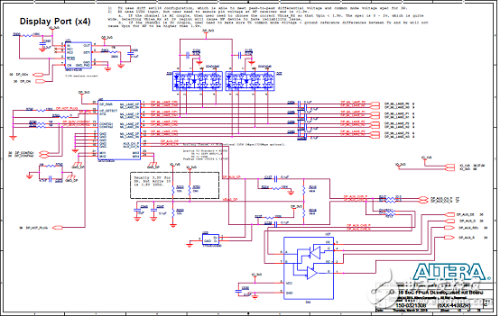
图15.Arria 10 SoC开发板电路图(12)
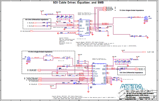
图16.Arria 10 SoC开发板电路图(13)
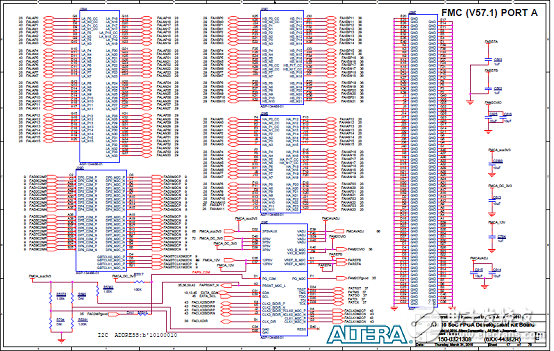
图17.Arria 10 SoC开发板电路图(14)
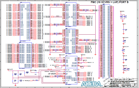
图18.Arria 10 SoC开发板电路图(15)
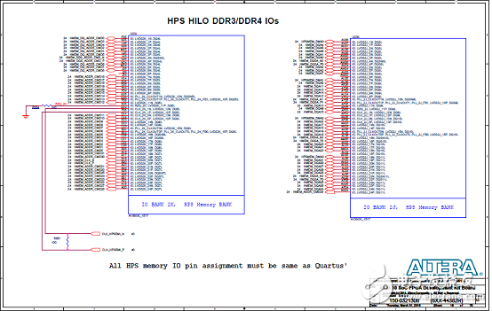
图19.Arria 10 SoC开发板电路图(16)
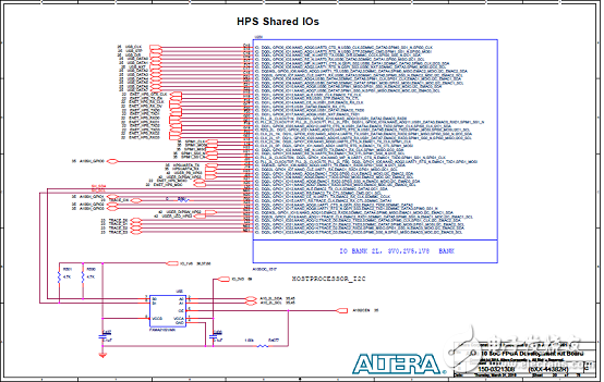
图20.Arria 10 SoC开发板电路图(17)
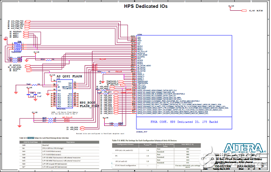
图21.Arria 10 SoC开发板电路图(18)
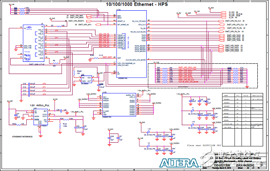
图22.Arria 10 SoC开发板电路图(19)
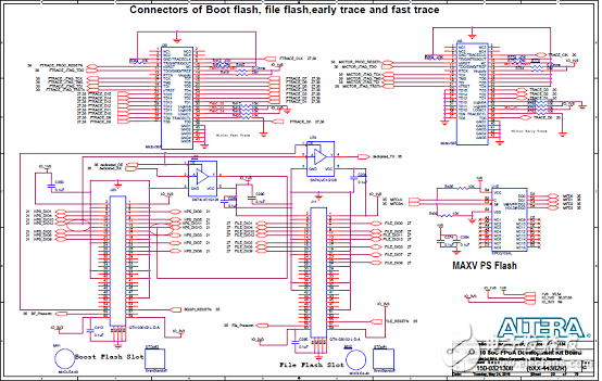
图23.Arria 10 SoC开发板电路图(20)
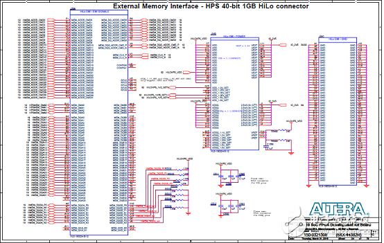
图24.Arria 10 SoC开发板电路图(21)
图25.Arria 10 SoC开发板电路图(22)
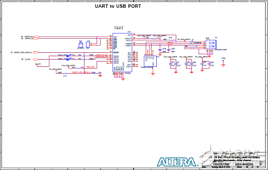
图26.Arria 10 SoC开发板电路图(23)
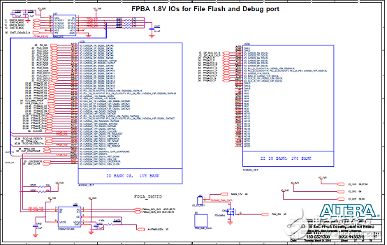
图27.Arria 10 SoC开发板电路图(24)
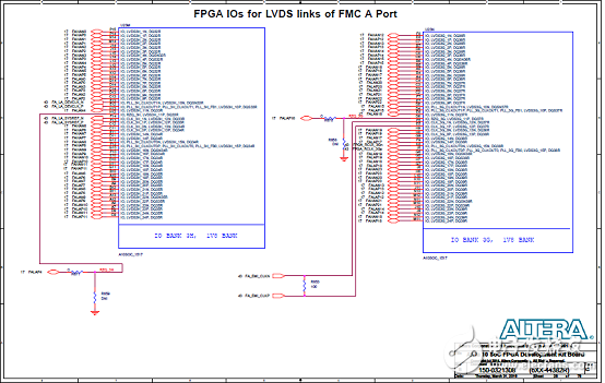
图28.Arria 10 SoC开发板电路图(25)
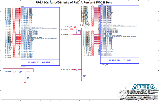
图29.Arria 10 SoC开发板电路图(26)
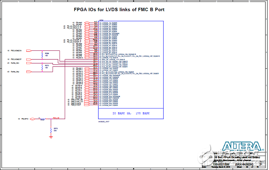
图30.Arria 10 SoC开发板电路图(27)
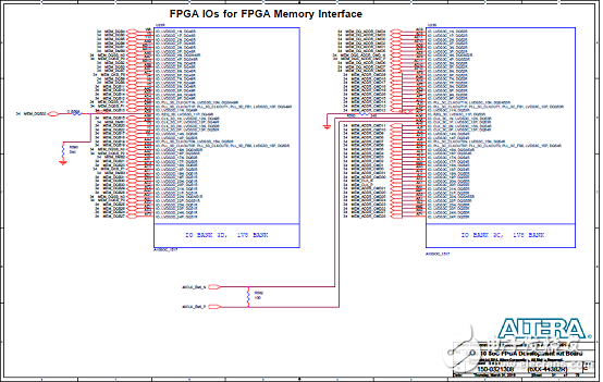
图31.Arria 10 SoC开发板电路图(28)
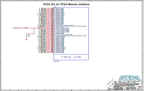
图32.Arria 10 SoC开发板电路图(29)
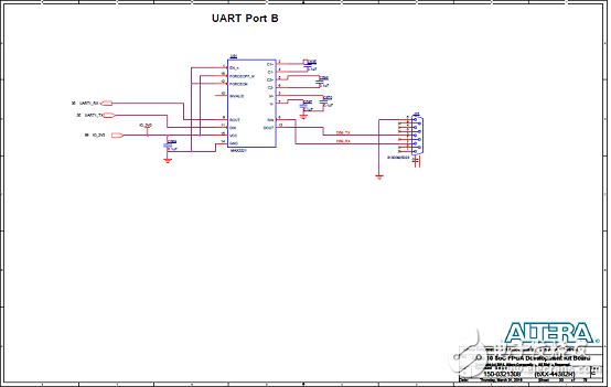
图33.Arria 10 SoC开发板电路图(30)
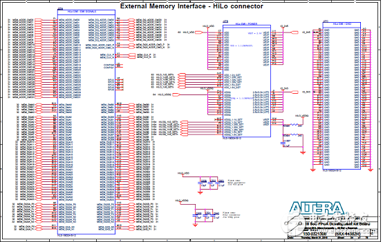
图34.Arria 10 SoC开发板电路图(31)
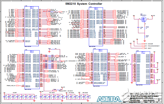
图35.Arria 10 SoC开发板电路图(32)
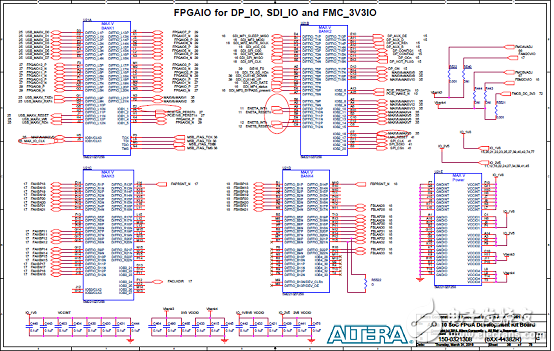
图36.Arria 10 SoC开发板电路图(33)
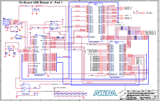
图37.Arria 10 SoC开发板电路图(34)
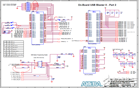
图38.Arria 10 SoC开发板电路图(35)
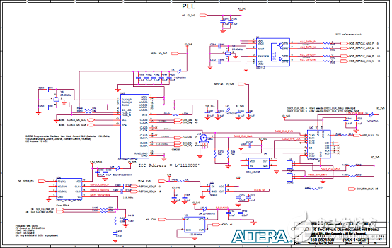
图39.Arria 10 SoC开发板电路图(36)
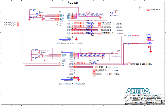
图40.Arria 10 SoC开发板电路图(37)
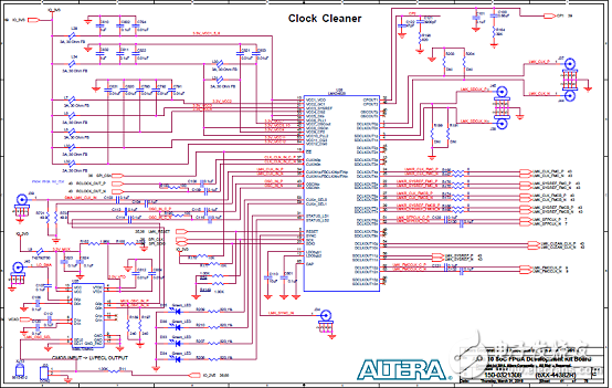
图41.Arria 10 SoC开发板电路图(38)
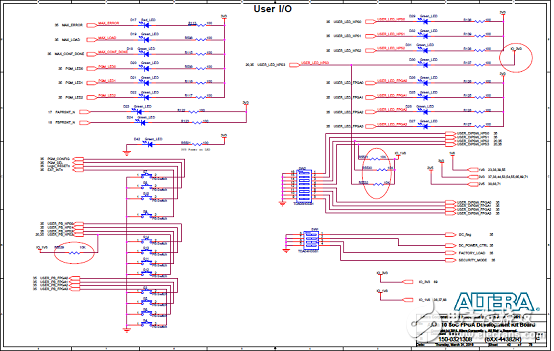
图42.Arria 10 SoC开发板电路图(39)
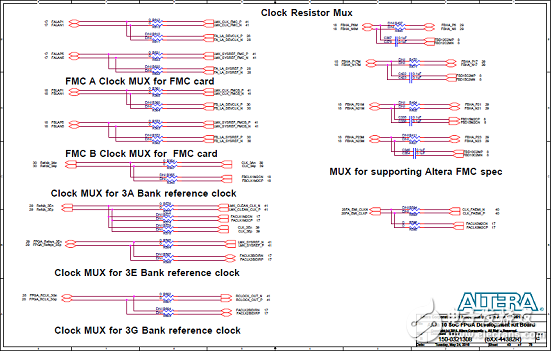
图43.Arria 10 SoC开发板电路图(40)
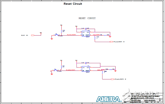
图44.Arria 10 SoC开发板电路图(41)
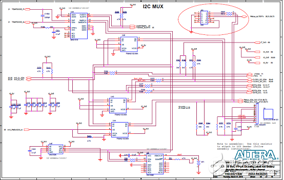
图45.Arria 10 SoC开发板电路图(42)
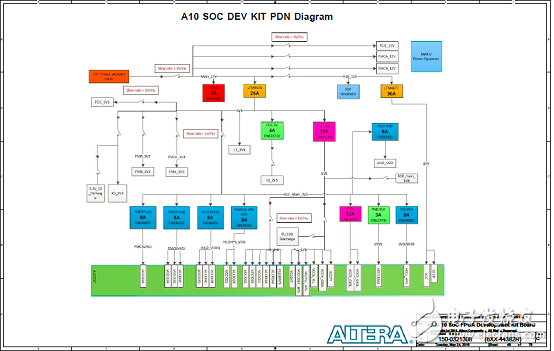
图46.Arria 10 SoC开发板电路图(43)
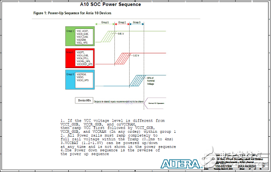
图47.Arria 10 SoC开发板电路图(44)
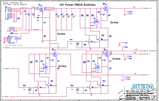
图48.Arria 10 SoC开发板电路图(45)
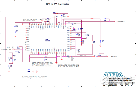
图49.Arria 10 SoC开发板电路图(46)
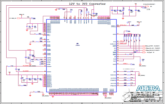
图50.Arria 10 SoC开发板电路图(47)
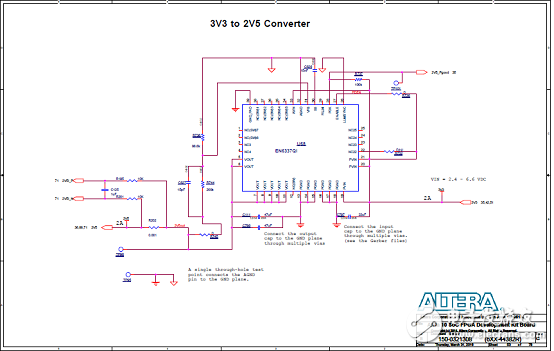
图51.Arria 10 SoC开发板电路图(48)
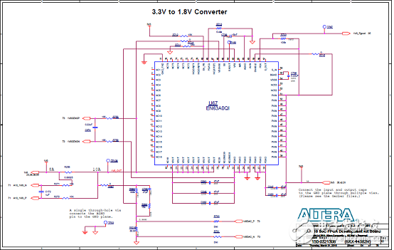
图52.Arria 10 SoC开发板电路图(49)
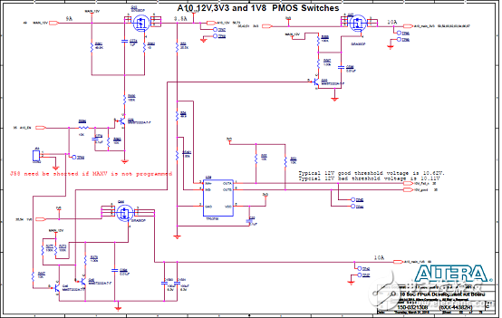
图53.Arria 10 SoC开发板电路图(50)
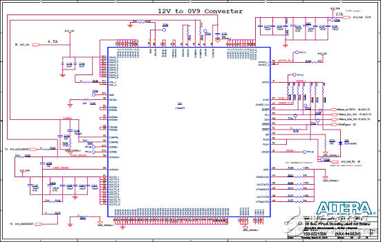
图54.Arria 10 SoC开发板电路图(51)
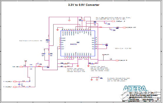
图55.Arria 10 SoC开发板电路图(52)
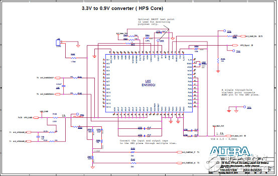
图56.Arria 10 SoC开发板电路图(53)
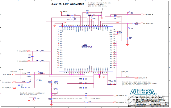
图57.Arria 10 SoC开发板电路图(54)
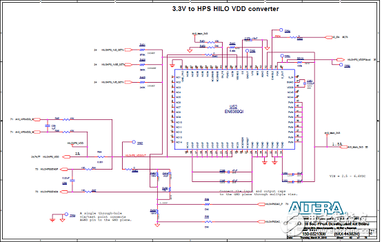
图58.Arria 10 SoC开发板电路图(55)
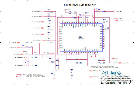
图59.Arria 10 SoC开发板电路图(56)
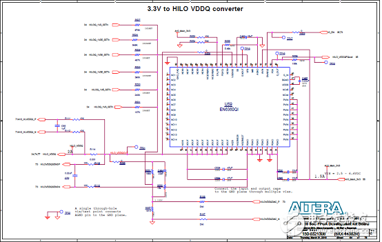
图60.Arria 10 SoC开发板电路图(57)
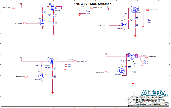
图61.Arria 10 SoC开发板电路图(58)
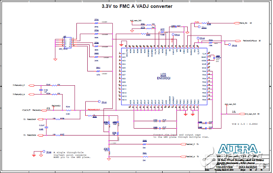
图62.Arria 10 SoC开发板电路图(59)
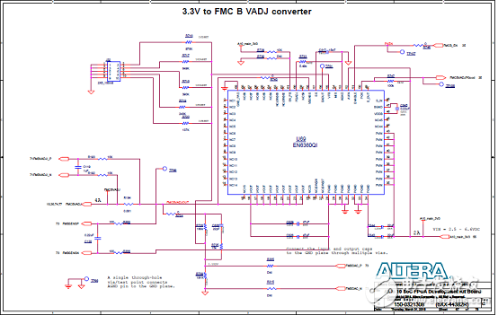
图63.Arria 10 SoC开发板电路图(60)
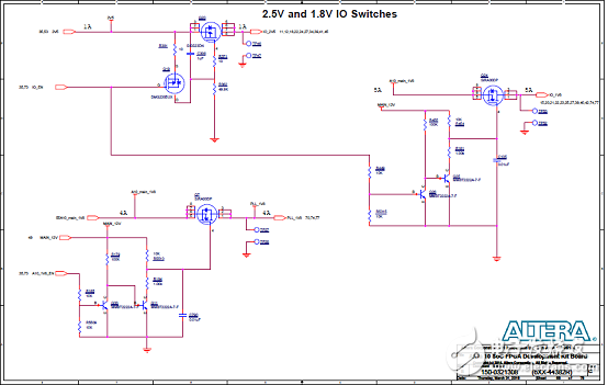
图64.Arria 10 SoC开发板电路图(61)
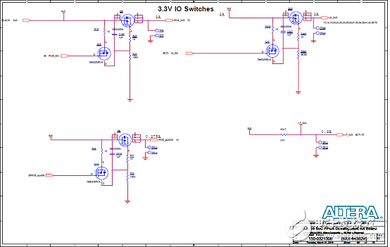
图65.Arria 10 SoC开发板电路图(62)
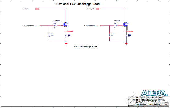
图66.Arria 10 SoC开发板电路图(63)
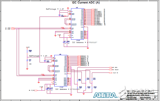
图67.Arria 10 SoC开发板电路图(64)
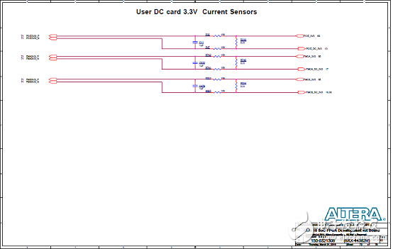
图68.Arria 10 SoC开发板电路图(65)
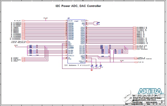
图69.Arria 10 SoC开发板电路图(66)
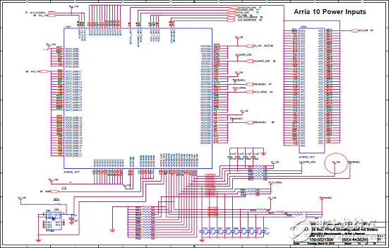
图70.Arria 10 SoC开发板电路图(67)
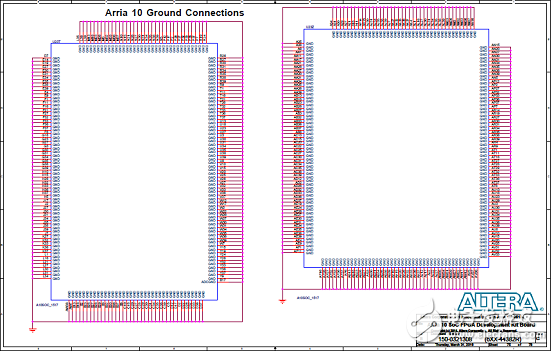
图71.Arria 10 SoC开发板电路图(68)
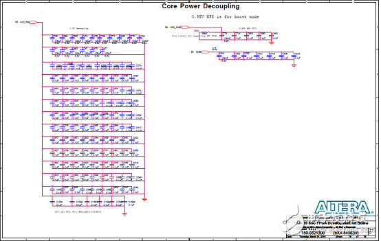
图72.Arria 10 SoC开发板电路图(69)
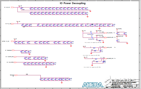
图73.Arria 10 SoC开发板电路图(70)
-
FPGA和SoC在设计中面临小尺寸和低成本挑战,如何解决2020-07-16 1445
-
FPGA构建高性能DSP2011-02-17 3312
-
Altera率先交付高性能28nm FPGA量产芯片2012-05-14 2932
-
面向GSPS ADC的低成本、高性能时钟解决方案包含BOM,PCB文件和组装图2018-08-16 2372
-
给Altera Arria 10 FPGA和Arria 10 SoC供电:经过测试和验证的电源管理解决方案2018-10-29 2883
-
Altera Arria V GX FPGA电源设计方案2018-12-04 2137
-
集成柔性功率器为FPGA和SoC设计降低成本2019-03-08 1920
-
Altera宣布为高性能FPGA提供高效的电源转换解决方案2018-02-11 5807
-
介绍Arria II GX的特点性能及应用2018-06-22 4674
-
英特尔Arria 10 SOC FPGA开发板硬件支持32位 DDR4 SDRAM2020-05-20 1987
-
Altera Arria V系列FPGA的电源解决方案2021-04-29 1049
-
英特尔Arria 10 FPGA的应用之路2021-05-31 4494
-
Arria 10 SoC确保系统设计满足现在和未来性能要求2022-06-30 1932
-
进阶的电动两轮车——更低成本,更高性能的BMS解决方案2022-10-28 1154
-
英特尔Arria 10器件:高性能与低功耗的完美结合2026-03-29 425
全部0条评论

快来发表一下你的评论吧 !
