

STM32L496AGI6及P-L496G-CELL02主要特性,框图和电路图
电子技术
描述
ST公司的STM32L496AGI6是基于高性能Arm® Cortex®-M4 32-位RISC核的超低功耗微控制器(MCU),工作频率高达80MHz.Cortex-M4核具有单精度浮点单元(FPU),支持所有的ARM单精度数据处理指令和数据类型,以及实现全套DSP指令和存储器保护单元(PMU),集成了1MB闪存,320KB SRAM以及USB OTG,LCD和DFSDM(外接Sigma-Delta调制器数字滤波器),电源电压1.71 V到3.6 V,可用于蜂窝通信和云计算.本文介绍了STM32L496AGI6主要特性,框图和时钟树,以及用于LTE IoT蜂窝到云的STM32 Discovery开发平台P-L496G-CELL02主要特性,框图和电路图.
The STM32 Discovery pack (P-L496G-CELL02) is a turnkey development platform for cellular and cloud technology based solutions. The pack contains an STM32L496AGI6- based low-power Discovery mother board and an STMod+ Cellular LTE IoT worldwide expansion board with antenna
The STM32L496xx devices are the ultra-low-power microcontrollers based on the high-performance Arm® Cortex®-M4 32-bit RISC core operating at a frequency of up to 80 MHz. The Cortex-M4 core features a Floating point unit (FPU) single precision which supports all Arm® single-precision data-processing instructions and data types. It also implements a full set of DSP instructions and a memory protection unit (MPU) which enhances application security.
The STM32L496xx devices embed high-speed memories (up to 1 Mbyte of Flash memory, 320 Kbyte of SRAM), a flexible external memory controller (FSMC) for static memories (for devices with packages of 100 pins and more), a Quad SPI flash memories interface (available on all packages) and an extensive range of enhanced I/Os and peripherals connected to two APB buses, two AHB buses and a 32-bit multi-AHB bus matrix.
The STM32L496xx devices embed several protection mechanisms for embedded Flash memory and SRAM: readout protection, write protection, proprietary code readout protection and Firewall.
The devices offer up to three fast 12-bit ADCs (5 Msps), two comparators, two operational amplifiers, two DAC channels, an internal voltage reference buffer, a low-power RTC, two general-purpose 32-bit timer, two 16-bit PWM timers dedicated to motor control, seven general-purpose 16-bit timers, and two 16-bit low-power timers. The devices support four digital filters for external sigma delta modulators (DFSDM).
In addition, up to 24 capacitive sensing channels are available. The devices also embed an integrated LCD driver 8x40 or 4x44, with internal step-up converter. They also feature standard and advanced communication interfaces.
The STM32L496xx operates in the -40 to +85 ℃ (+105 ℃ junction), -40 to +125 ℃ (+130 ℃ junction) temperature ranges from a 1.71 to 3.6 V VDD power supply when using internal LDO regulator and a 1.05 to 1.32V VDD12 power supply when using external SMPS supply. A comprehensive set of power-saving modes allows the design of low-power applications.
Some independent power supplies are supported: analog independent supply input for ADC, DAC, OPAMPs and comparators, 3.3 V dedicated supply input for USB and up to 14 I/Os can be supplied independently down to 1.08V. A VBAT input allows to backup the RTC and backup registers. Dedicated VDD12 power supplies can be used to bypass the internal LDO regulator when connected to an external SMPS.
• Four I2Cs
• Three SPIs
• Three USARTs, two UARTs and one Low-Power UART.
• Two SAIs (Serial Audio Interfaces)
• One SDMMC
• Two CAN
• One USB OTG full-speed
• One SWPMI (Single Wire protocol Master Interface)
• Camera interface
• DMA2D controller
STM32L496AGI6主要特性:
• Ultra-low-power with FlexPowerControl
– 1.71 V to 3.6 V power supply
– -40 °C to 85/125 °C temperature range
– 320 nA in VBAT mode: supply for RTC and 32x32-bit backup registers
– 25 nA Shutdown mode (5 wakeup pins)
– 108 nA Standby mode (5 wakeup pins)
– 426 nA Standby mode with RTC
– 2.57 μA Stop 2 mode, 2.86 μA Stop 2 with RTC
– 91 μA/MHz run mode (LDO Mode)
– 37 μA/MHz run mode (@3.3 V SMPS Mode)
– Batch acquisition mode (BAM)
– 5 μs wakeup from Stop mode
– Brown out reset (BOR) in all modes except shutdown
– Interconnect matrix
• Core: Arm® 32-bit Cortex®-M4 CPU with FPU, Adaptive real-time accelerator (ART Accelerator™) allowing 0-wait-state execution from Flash memory, frequency up to 80 MHz, MPU, 100 DMIPS and DSP instructions
• Performance benchmark
– 1.25 DMIPS/MHz (Drystone 2.1)
– 273.55 Coremark® (3.42 Coremark/MHz @ 80 MHz)
• Energy benchmark
– 279 ULPMark™ CP score
– 80.2 ULPMark™ PP score
• 16 x timers: 2 x 16-bit advanced motor-control, 2 x 32-bit and 5 x 16-bit general purpose, 2 x 16-bit basic, 2 x low-power 16-bit timers (available in Stop mode), 2 x watchdogs, SysTick timer
• RTC with HW calendar, alarms and calibration
• Up to 136 fast I/Os, most 5 V-tolerant, up to 14 I/Os with independent supply down to 1.08 V
• Dedicated Chrom-ART Accelerator™ for enhanced graphic content creation (DMA2D)
• 8- to 14-bit camera interface up to 32 MHz (black&white) or 10 MHz (color)
• Memories
– Up to 1 MB Flash, 2 banks read-while-write, proprietary code readout protection
– 320 KB of SRAM including 64 KB with hardware parity check
– External memory interface for static memories supporting SRAM, PSRAM, NOR and NAND memories
– Dual-flash Quad SPI memory interface
• Clock Sources
– 4 to 48 MHz crystal oscillator
– 32 kHz crystal oscillator for RTC (LSE)
– Internal 16 MHz factory-trimmed RC (±1%)
– Internal low-power 32 kHz RC (±5%)
– Internal multispeed 100 kHz to 48 MHz oscillator, auto-trimmed by LSE (better than ±0.25% accuracy)
– Internal 48 MHz with clock recovery
– 3 PLLs for system clock, USB, audio, ADC
• LCD 8 × 40 or 4 × 44 with step-up converter
• Up to 24 capacitive sensing channels: support touchkey, linear and rotary touch sensors
• 4 x digital filters for sigma delta modulator
• Rich analog peripherals (independent supply)
– 3 × 12-bit ADC 5 Msps, up to 16-bit with hardware oversampling, 200 μA/Msps
– 2 x 12-bit DAC, low-power sample and hold
– 2 x operational amplifiers with built-in PGA
– 2 x ultra-low-power comparators
• 20 x communication interfaces
– USB OTG 2.0 full-speed, LPM and BCD
– 2 x SAIs (serial audio interface)
– 4 x I2C FM+(1 Mbit/s), SMBus/PMBus
– 5 x U(S)ARTs (ISO 7816, LIN, IrDA, modem)
– 1 x LPUART
– 3 x SPIs (4 x SPIs with the Quad SPI)
– 2 x CAN (2.0B Active) and SDMMC
– SWPMI single wire protocol master I/F
– IRTIM (Infrared interface)
• 14-channel DMA controller
• True random number generator
• CRC calculation unit, 96-bit unique ID
• Development support: serial wire debug (SWD), JTAG, Embedded Trace Macrocell™

图1.STM32L496AGI6框图

图2.STM32L496AGI6时钟树
用于LTE IoT蜂窝到云的STM32 Discovery开发平台P-L496G-CELL02
The STM32 Discovery pack (P-L496G-CELL02) is a turnkey development platform for cellular and cloud technology based solutions. The pack contains an STM32L496AGI6- based low-power Discovery mother board and anSTMod+ Cellular LTE IoT worldwide expansion board with antenna.

图3.STM32 Discovery开发平台P-L496G-CELL02外形图
STM32 Discovery开发平台P-L496G-CELL02主要特性:
• STM32L496AGI6 Arm®-based microcontroller featuring 1 Mbyte of Flash memory and 320 Kbytes of RAM in a UFBGA169 package
• USB OTG HS
• On-board current measurement
• SAI Audio CODEC
• ST-MEMS digital microphones
• 8-Mbit PSRAM
• 2 user LEDs
• 1 user and 1 reset push-buttons
• 4-direction joystick with selection button
• Board connectors:
– Camera 8 bit
– USB with Micro-AB
– Stereo headset jack including analog microphone input
– microSD™ card
• Board expansion connectors:
– Arduino™ Uno V3
– STMod+
• Board expansion features: –
Quectel BG96 worldwide cellular modem LTE Cat M1/Cat NB1/EGPRS module 300 kbps downlink, 375 kbps uplink
– Modem reset red LED and modem signaling green LED
– Switchable SIM interface, eSIM and micro SIM
– Pulse SMA antenna for frequency ranges: 824 / 900 / 1800 / 1900 / 2100 MHz This antenna may not be suitable for your LTE Band, please use at that time the SPDA24700 antenna from Pulse
• Flexible power-supply options: ST-LINK, USB VBUS, or external sources
• On-board ST-LINK/V2-1 SWD,TAG debugger/programmer with USB re-enumeration capability: mass storage, virtual COM port and debug port
• Comprehensive free software libraries and examples available with the STM32Cube package
• Support of a wide choice of integrated development environments (IDEs) including IAR™, Keil®, GCC-based IDEs

图4.STM32 Discovery开发平台P-L496G-CELL02外形图:主板和扩展LTE IoT调制解调器

图5.STM32 Discovery开发平台P-L496G-CELL02外形图(底面)

图6.STM32 Discovery开发平台P-L496G-CELL02电路图(1)

图7.STM32 Discovery开发平台P-L496G-CELL02电路图(2):扩展板调制解调器

图8.STM32 Discovery开发平台P-L496G-CELL02电路图(3):扩展板SIM
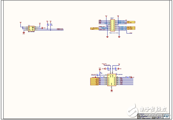
图9.STM32 Discovery开发平台P-L496G-CELL02电路图(4):扩展板STMod+

图10.STM32 Discovery开发平台P-L496G-CELL02电路图(5):扩展板电源
-
AT命令使用stm32l496模块没有响应怎么解决?2023-01-10 422
-
STM32L496QGI6P不同生产“日期代码”表现不同是这样嘛?2023-01-09 543
-
MCU (STM32L496VGYXP) 内部闪存报错怎么解决?2022-12-05 728
-
STM32L496xx/STM32L4A6xx设备勘误表2022-11-30 478
-
ES0335_STM32L496xx和STM32L4A6xx单片机的局限性2022-11-23 854
-
UM2145_STM32L496探索套件STM32CubeL4演示固件2022-11-22 648
-
AN4822_STM32L476xx、486xx和STM32L496xx、4A6xx微控制器之间的移植2022-11-21 1047
-
基于NUCLEO-L496ZG-P微控制器的参考设计2021-07-09 745
-
STM32L4P5AGI6 STMicroelectronics STM32L4P5/STM32L4Q5 32位微控制器 (MCU)2020-11-06 879
-
UM2322用于2G和3G蜂窝至云技术的STM32探索包的详细资料说明2018-11-30 1346
-
介绍STM32L496G开发套件的特点及应用2018-07-03 5964
全部0条评论

快来发表一下你的评论吧 !
