

ADI AD4002 18位2 MSPS SAR ADC评估方案详解
电子说
描述
ADI公司的AD4002是低噪声低功耗高速18 位取样频率2 MSPS 精密逐次逼近寄存器 (SAR) 模数转换器 (ADC),集成了多种易用特性,可以减少信号链功率,降低信号链复杂性以及实现更高的通道密度.INL最大为±3.2 LSB,18位不丢码,10kSPS时功耗70uW,2MSPS时为14mW,SNR在1kHz,VREF = 5 V时为95dB,THD在1 kHz,VREF = 5 V时为-125dB,主要用在自动测试设备,机器自动化,医疗器械,电池供电设备和精密数据采集系统。本文介绍了AD4002/AD4006/AD4010主要特性,功能框图,ADC简化电路图,典型应用框图,以及评估板EVAL-AD400xFMCZ主要特性,框图,电路图,材料清单和PCB设计图。
The AD4002/AD4006/AD4010 are low noise, low power, high speed, 18-bit, precision successive approximation register (SAR) analog-to-digital converters (ADCs)。 The AD4002, AD4006, and AD4010 offer 2 MSPS, 1 MSPS, and 500 kSPS throughputs, respectively. They incorporate ease of use features that reduce signal chain power consumption, reduce signal chain complexity, and enable higher channel density. The high-Z mode, coupled with a long acquisition phase, eliminates the need for a dedicated high power, high speed ADC driver, thus broadening the range of low power precision amplifiers that can drive these ADCs directly while still achieving optimum performance. The input span com-pression feature enables the ADC driver amplifier and the ADC to operate off common supply rails without the need for a negative supply while preserving the full ADC code range. The low serial peripheral interface (SPI) clock rate requirement reduces the digital input/output power consumption, broadens processor options, and simplifies the task of sending data across digital isolation.
Operating from a 1.8 V supply, the AD4002/AD4006/AD4010 sample an analog input (IN+) from 0 V to VREF with respect to a ground sense (IN−) with VREF ranging from 2.4 V to 5.1 V. The AD4002 consumes only 14 mW at 2 MSPS with a minimum SCK rate of 75 MHz in turbo mode; the AD4006 consumes only 7 mW at 1 MSPS; and the AD4010 consumes only 3.5 mW at 500 kSPS. The AD4002/AD4006/AD4010 all achieve ±3.2 LSB integral nonlinearity error (INL) maximum, no missing codes at 18 bits, and 95 dB signal-to-noise ratio (SNR) for an input frequency (fIN) of 1 kHz. The reference voltage is applied externally and can be set independently of the supply voltage.
The SPI-compatible versatile serial interface features seven different modes including the ability, using the SDI input, to daisy-chain several ADCs on a single 3-wire bus, and provides an optional busy indicator. The AD4002/AD4006/AD4010 are compatible with 1.8 V, 2.5 V, 3 V, and 5 V logic, using the separate VIO supply.
The AD4002/AD4006 are available in a 10-lead MSOP and 10-lead LFCSP, and the AD4010 is available in a 10-lead LFCSP, with operation specified from −40℃ to +125℃。 The devices are pin compatible with the 18-bit, 2 MSPS AD4003 (see Table 8)。
AD4002/AD4006/AD4010主要特性:
Throughput: 2 MSPS/1 MSPS/500 kSPS options
INL: ±3.2 LSB maximum
Guaranteed 18-bit, no missing codes
Low power: 70 μW at 10 kSPS, 14 mW at 2 MSPS (total)
9.75 mW at 2 MSPS, 4.9 mW at 1 MSPS, 2.5 mW at 500 kSPS (VDD only)
SNR: 95 dB typical at 1 kHz, VREF = 5 V; 95 dB typical at 100 kHz
THD: −125 dB typical at 1 kHz, VREF = 5 V; −108 dB typical at 100 kHz
Ease of use features reduce system power and complexity
Input overvoltage clamp circuit
Reduced nonlinear input charge kickback
High-Z mode
Long acquisition phase
Input span compression
Fast conversion time allows low SPI clock rates
SPI-programmable modes, read/write capability, status word
Pseudo differential (single-ended) analog input range
0 V to VREF with VREF from 2.4 V to 5.1 V
Single 1.8 V supply operation with 1.71 V to 5.5 V logic interface
SAR architecture: no latency/pipeline delay, valid first conversion
First conversion accurate
Guaranteed operation: −40℃ to +125℃
SPI-/QSPI-/MICROWIRE-/DSP-compatible serial interface
Ability to daisy-chain multiple ADCs and busy indicator
10-lead packages: 3 mm × 3 mm LFCSP, 3 mm × 4.90 mm MSOP
AD4002/AD4006/AD4010应用:
Automatic test equipment
Machine automation
Medical equipment
Battery-powered equipment
Precision data acquisition systems
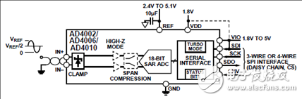
图1.AD4002/AD4006/AD4010功能框图
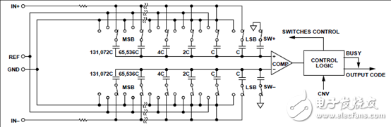
图2.ADC简化电路图
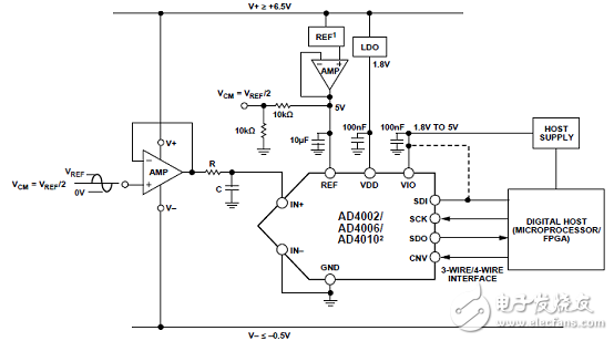
图3.AD4002/AD4006/AD4010多个电源典型应用框图
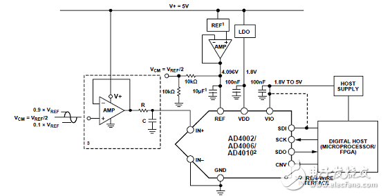
图4.AD4002/AD4006/AD4010单电源典型应用框图
评估板EVAL-AD400xFMCZ
The AD4000/AD4001/AD4002/AD4003/AD4020 family evaluation board covers the ease of use, 16-/18-/20-bit, precision successive approximation register (SAR) analog-to-digital converters (ADCs)。 The AD4000/AD4001/AD4002/ AD4003/AD4020 are low power, 16-bit/18-bit/20-bit, precision SAR ADCs that offer very high performance with throughputs up to 2 MSPS (1.8 MSPS for the AD4020)。 The evaluation board is designed to demonstrate the performance of the AD4000/AD4001/AD4002/AD4003/AD4020 family of ADCs and to provide an easy to understand interface for a variety of system applications. A full description of these products is available in their respective data sheets, which must be consulted when using this evaluation board.
The EVAL-AD4000FMCZ/EVAL-AD4001FMCZ/EVAL-AD4002FMCZ/EVAL-AD4003FMCZ/EVAL-AD4020FMCZ evaluation boards (see Figure 1) are ideal for use with the Analog Devices, Inc., high speed system demonstration platform (EVAL-SDP-CH1Z)。 These evaluation boards interface to the SDP-H1 board via a 120-pin connector. SMA connectors, JP2 and JP3, are provided for the low noise analog signal source.
On-board components include a high precision buffered band gap 5.0 V reference (the ADR4550), a reference buffer (the ADA4807-1), a common-mode buffer (the ADA4807-1), a signal conditioning circuit with two op amps (the ADA4807-1), and a power supply to derive the necessary voltage levels to supply all voltage needs.
The EVAL-AD4000FMCZ, EVAL-AD4001FMCZ, EVAL-AD4002FMCZ, and EVAL-AD4003FMCZ are populated with the AD4000, AD4001, AD4002, and AD4003, respectively. However, these boards can be used to evaluate the performance of the AD4004, AD4005, AD4006, AD4007, AD4008, AD4010, and AD4011 by limiting the sample rate in the evaluation software to the maximum sample rate of the specific ADC. For example, the AD4000 on the EVAL-AD4000FMCZ can be used to evaluate the performance of the AD4004 if the sample rate is limited to 1 MSPS. See the data sheet of each product for its corresponding evaluation board.
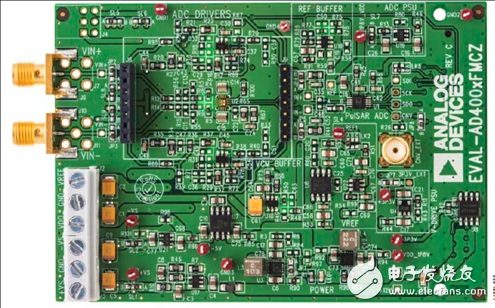
图5.评估板EVAL-AD400xFMCZ外形图
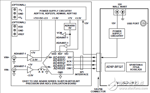
图6.评估板EVAL-AD400xFMCZ简化框图
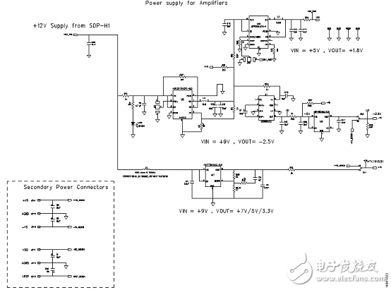
图7.评估板EVAL-AD400xFMCZ电路图(1):电源
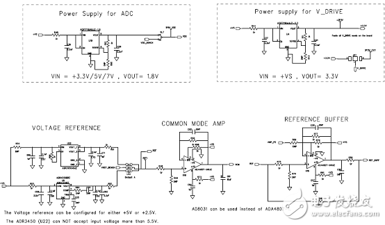
图8.评估板EVAL-AD400xFMCZ电路图(2):基准电压,共模和基准缓冲器
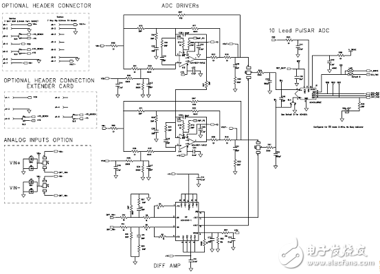
图9.评估板EVAL-AD400xFMCZ电路图(3):ADC驱动器和ADC
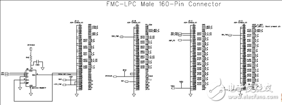
图10.评估板EVAL-AD400xFMCZ电路图(4):SDP-H1连接器和胶合逻辑
评估板EVAL-AD400xFMCZ材料清单:
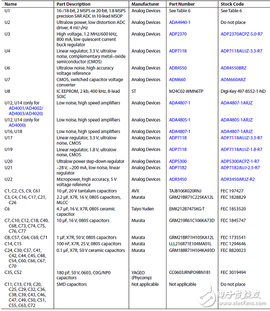
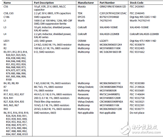
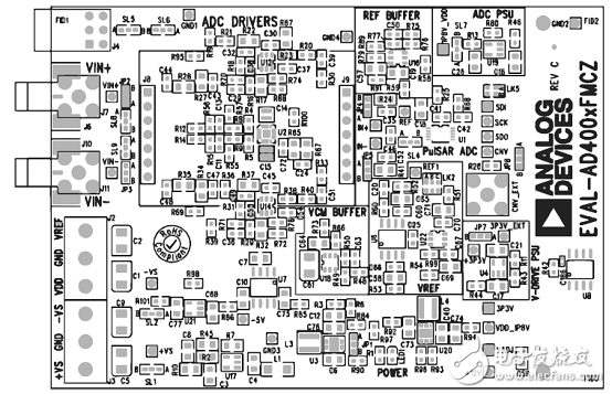
图11.评估板EVAL-AD400xFMCZ PCB设计图:顶层丝印
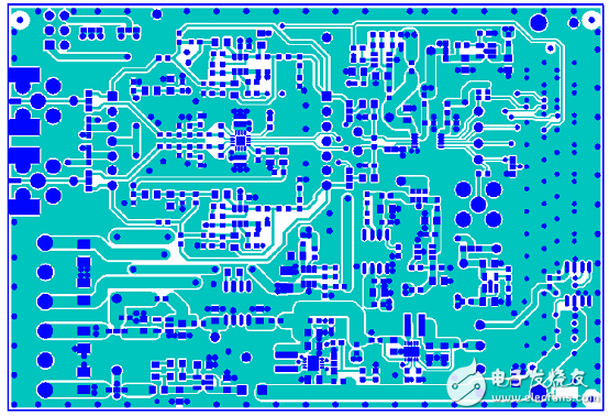
图12.评估板EVAL-AD400xFMCZ PCB设计图:层1
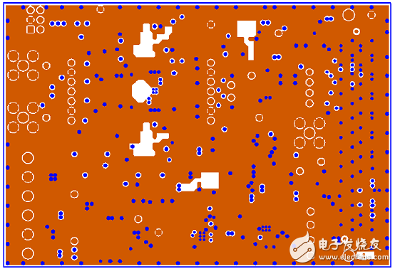
图13.评估板EVAL-AD400xFMCZ PCB设计图:层2
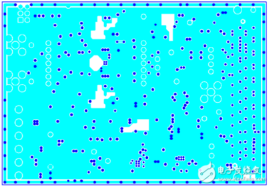
图14.评估板EVAL-AD400xFMCZ PCB设计图:层3
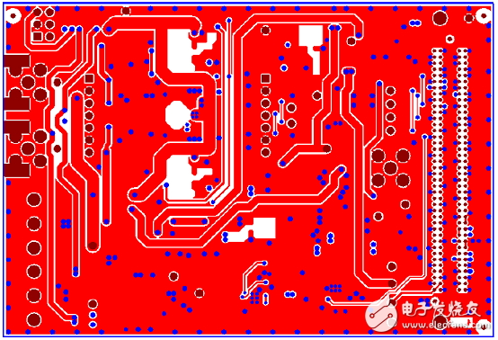
图15.评估板EVAL-AD400xFMCZ PCB设计图:层4
-
18位2MSPS SAR ADC AD7641:高性能数据转换的理想之选2026-04-02 555
-
18位15Msps SAR ADC LTC2387-18:性能卓越,应用广泛2026-03-31 651
-
AD4002/AD4006/AD4010:高精度SAR ADC的卓越之选2026-03-27 363
-
EVAL-AD7482CB:3 MSPS评估板,12位SAR ADC数据表2021-05-20 948
-
18位、15Msps SAR ADC,无周期延迟2021-05-18 999
-
AD7484:3 MSPS,14位SAR ADC数据Sheet2021-05-10 1136
-
AD4002/AD4006/AD4010:18位,2 MSPS/1 MSPS/500 kSPS,精度,伪差分,SAR ADC数据表2021-05-09 1030
-
双16位5Msps SAR ADC2021-04-30 1128
-
AD7482:3 MSPS,12位SAR ADC数据Sheet2021-04-29 1011
-
18位1Msps 8通道SAR ADC2021-04-17 1061
-
AD7641:18位,2 MSPS SAR ADC数据Sheet2021-04-16 1106
-
18 位、2.5Msps、无延迟 SAR ADC可实现 99.8dB SNR 及灵活的模拟输入范围2021-03-21 1129
-
18 位、1.6Msps、串行 SAR ADC实现业界领先的 101dB SNR 性能2021-03-19 874
全部0条评论

快来发表一下你的评论吧 !
