

AD8452主要特性_框图以及应用电路
电子说
描述
ADI公司的AD8452是具有透明和自动切换特性的 CC 和 CV 电池测试和化成模块,组合了精密模拟前端(AFE)控制器和开关电源(SMPS),脉宽调制器(PWM)驱动器,精密仪表放大器(in-amp)测量电池充电/放电电流精度优于±0.1%,电流感应仪器放大器增益66 V/V,电压感应差分放大器增益0.4 V/V,失调电压漂移<0.6 μV/℃,增益漂移<3 ppm/℃,同步输出或输入,相移可调,可编程软启动,主要用在电池化成和测试,具有循环效能的高效电池测试系统和电池调理(充电和放电)系统.本文介绍了AD8452主要特性,框图,应用电路,评估板AD8452-EVALZ主要特性,框图,电路图,材料清单和PCB设计图.此外还介绍了相应的AD8452电池测试和化成评估板(电源板和模拟接口板)主要特性,框图,电路图,材料清单和PCB设计图.
The AD8452 combines a precision analog front-end controller and switch mode power supply (SMPS), pulse-width modulator (PWM) driver into a single silicon platform for high volume battery testing and formation manufacturing. A precision instrumentation amplifier (in-amp) measures the battery charge/ discharge current to better than ±0.1% accuracy, while an equally accurate difference amplifier measures the battery voltage. Internal laser trimmed resistor networks establish the in-amp and difference amplifier gains (66 V/V and 0.4 V/V, respectively), and stabilize the AD8452 performance across the rated operating temperature range. Desired battery cycling current and voltage levels are established by applying precise control voltages to the ISET and VSET inputs. Actual charge and discharge current levels are sensed (usually by a high power, highly accurate shunt resistor) whose value is carefully selected according to system parameters. Switching between constant current (CC) and constant voltage (CV) loop integration is instantaneous, automatic, and completely transparent to the observer. A logic high at the MODE input selects the charge or discharge mode (high for charge, low for discharge). The AD8452 simplifies designs by providing excellent performance, functionality, and overall reliability in a space saving 48-lead, 7 mm × 7 mm × 1.4 mm LQFP package rated for operation at temperatures from −40℃ to +85℃.
AD8452主要特性:
CC and CV battery test and formation modes with transparent and automatic switchover, for systems of 20 Ah or less
Precise measurement of voltage and current
Independent feedback control blocks
Highly accurate, factory trimmed instrumentation and differential amplifiers In-amp for current sense gain: 66 V/V Difference amplifier for voltage sense gain: 0.4 V/V
Stable over temperature: offset voltage drift <0.6 μV/℃ (maximum)
Gain drift: <3 ppm/℃ (maximum) Current sense CMRR: 120 dB minimum
Popular SMPS control for charge/discharge
High PWM linearity with internal ramp voltage
50 kHz to 300 kHz user controlled switching frequency
Synchronization output or input with adjustable phase shift
Programmable soft start
AD8452应用:
Battery formation and testing
High efficiency battery test systems with recycle capability
Battery conditioning (charging and discharging) systems
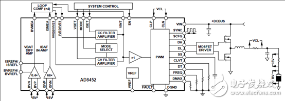
图1.AD8452功能框图
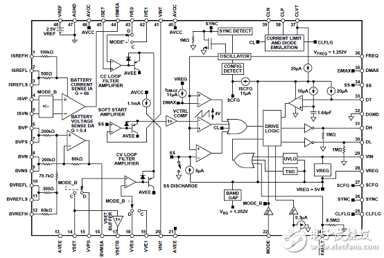
图2.AD8452详细框图
图3.AD8452锂电池和测试信号通路图
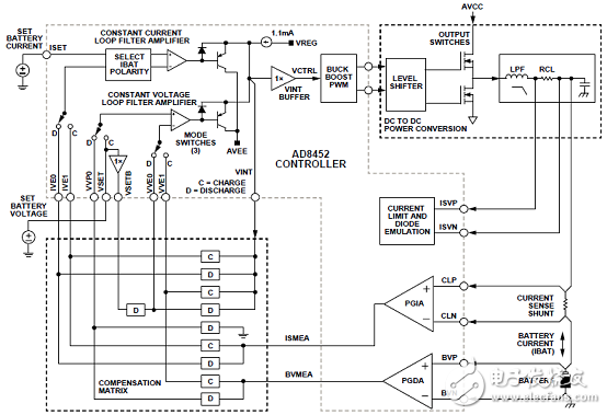
图4.AD8452锂电池测试和化成系统完整信号通路图
AD8452通用评估板AD8452-EVALZ
The AD8452-EVALZ is a platform for the AD8452, designed for investigation of the AD8452 analog and pulse-width modulation (PWM) features and performance without the added complica- tions of a driver and/or switch mode power supply (SMPS) design. For convenience, a precision 5 V reference IC and four trim pots are built in to the evaluation board, for driving the battery current and voltage ISET and VSET inputs. All device pins are accessible with test loops or probe landings. At the same time, the AD8452-EVALZ has the flexibility to interface and drive a typical half bridge inductor input SMPS with output levels in the 1 A to 15 A range. SMPS and associated components are specified and sourced by the user. The AD8452 is intended for use as the core controller for commercial battery test and formation systems. Its advanced miniaturization and extraordinarily high level of analog precision meet the challenge of mass production of high energy density storage lithium ion packs for transportation and energy storage in homes.
评估板AD8452-EVALZ主要特性:
Pin accessible, standalone AD8452
Simplified operation: connect a power supply and scope and start looking at waveforms
On-board precision 5 V reference included for accurate gain measurements
Factory tested
Four optional control loops available but not necessary for operation; may be bypassed as desired
Safe: only low power circuitry is present; no accidental power discharges
图5.评估板AD8452-EVALZ外形图
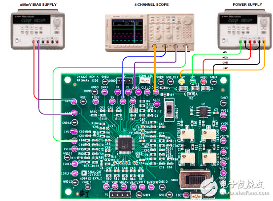
图6.评估板AD8452-EVALZ测试建立图
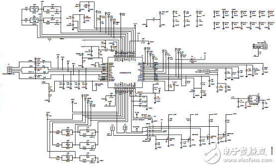
图7.评估板AD8452-EVALZ电路图
评估板AD8452-EVALZ材料清单:
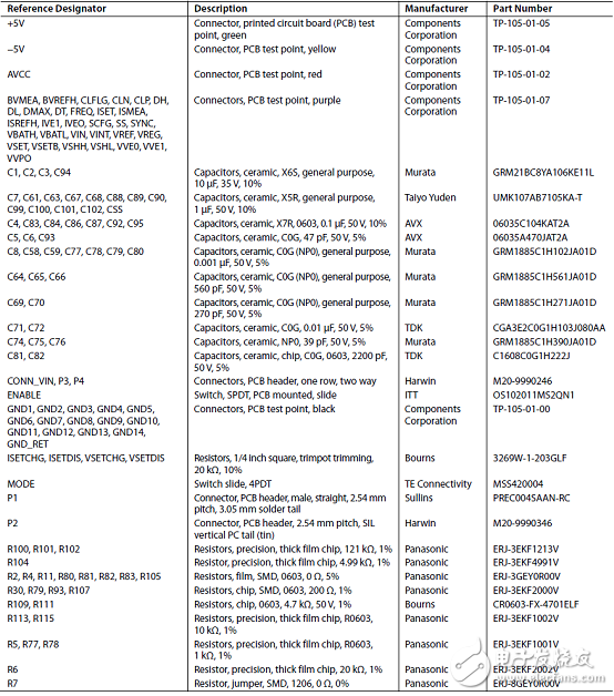
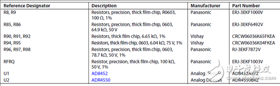

图8.评估板AD8452-EVALZ PCB丝印图
图9.评估板AD8452-EVALZ PCB顶层(元件面)布局图
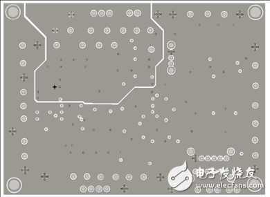
图10.评估板AD8452-EVALZ PCB设计图:层2-地
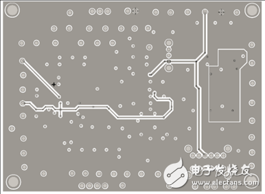
图11.评估板AD8452-EVALZ PCB设计图:层3-电源
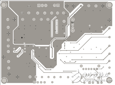
图12.评估板AD8452-EVALZ PCB设计图:底层-铜
AD8452电池测试和化成评估板
The AD8452 system demo evaluation kit is a recommended starting point for users building battery formation and test equipment based on the Analog Devices, Inc., AD8452 precision analog front end and pulse-width modulation (PWM) controller. The evaluation kit includes an analog interface board and a power module board.
In addition to the AD8452, the analog interface board also includes an AD5689R 16-bit, precision digital-to-analog converter (DAC) to set the current and voltage set points, and an AD7173-8 24-bit, Σ-Δ analog-to-digital converter (ADC) to monitor the battery voltage and current.
The analog interface board includes built-in voltage regulators so that it can be powered either from the bus power inputs or directly from a 15 V dc supply through a screw terminal connector.
The analog interface board connects to the Analog Devices System Demonstration Platform (SDP-S) through a 120-pin connector. The SDP-S board connects to the user interface software through the USB port, allowing the user to set the current and voltage set point as well as the mode of operation (charge or discharge). In addition, the user can monitor the battery voltage and current by reading the data output from the AD7173-8.
The analog interface board connects to the power module board through three multipin headers. This modular approach allows the user to design and test their own power module boards, designed for the current output range in their end applications, with the analog interface board of this reference design.
The standard power module board supports charge and discharge currents of up to 10 A. It includes the power metal-oxide semiconductor field effect transistors (MOSFETs), the inductor, and the input and output capacitors required to implement a buck or boost regulator, depending on the operating mode.
Full specifications of the AD8452 are available in the product data sheet, which must be consulted in conjunction with this user guide when working with the evaluation kit.
AD8452电池测试和化成评估板主要特性:
Fully functional Li-Ion cell formation and testing similar to real-world manufacturing equipment
Ability to charge and discharge batteries under constant current and constant voltage control
Energy recycling from discharging battery into a dc bus
Full featured system evaluation board based on the AD8452
PC software for control and monitoring of system parameters
Compatible with the System Demonstration Platform, SDP-S (EVAL-SDP-CS1Z)
AD8452电池测试和化成评估板包括:
Analog interface board
Power module board (10 V to 20 V dc operating range)
SDP-S board for data transfer to PC
Standard USB A to Mini-B USB cable
Printed user guide
Evaluation kit software CD
图13.AD8452电池测试和化成评估板外形图:上:电源模块;下:模拟接口板
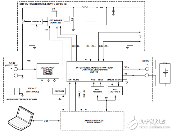
图14.AD8452电池测试和化成评估板系统框图
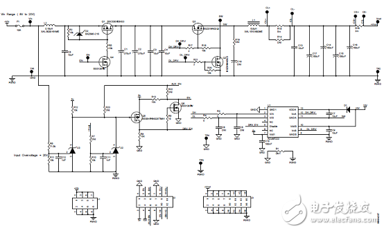
图15.AD8452电池测试和化成评估板电源模块电路图
电源模块材料清单:
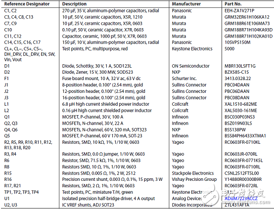
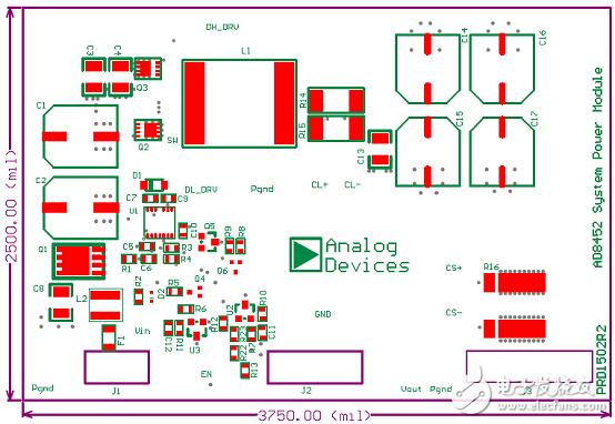
图16.电源模块PCB设计图:顶层丝印
图17.电源模块PCB设计图:顶层布局
图18.电源模块PCB设计图:层2布局
图19.电源模块PCB设计图:层3布局
图20.电源模块PCB设计图:底层布局
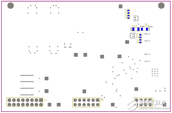
图21.电源模块PCB设计图:底层丝印
图22.电源模块PCB综合设计图
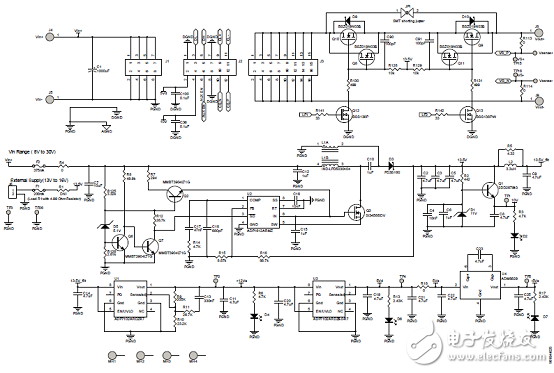
图23.模拟接口板电路(1):电源连接器和辅助电源
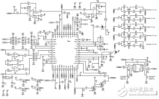
图24.模拟接口板电路(2):AD8452和补偿网络
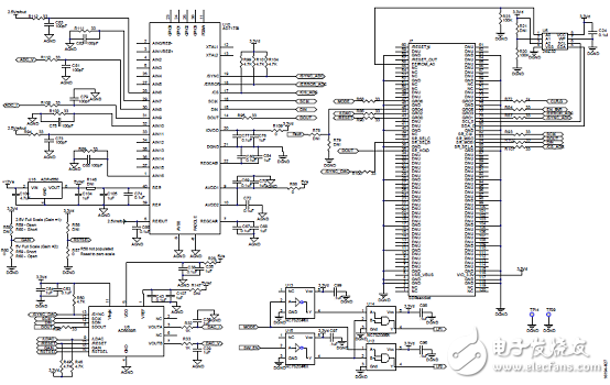
图25.模拟接口板电路(3):ADC,DAC和SDP连接器
模拟接口板材料清单:
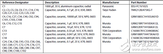
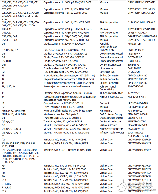
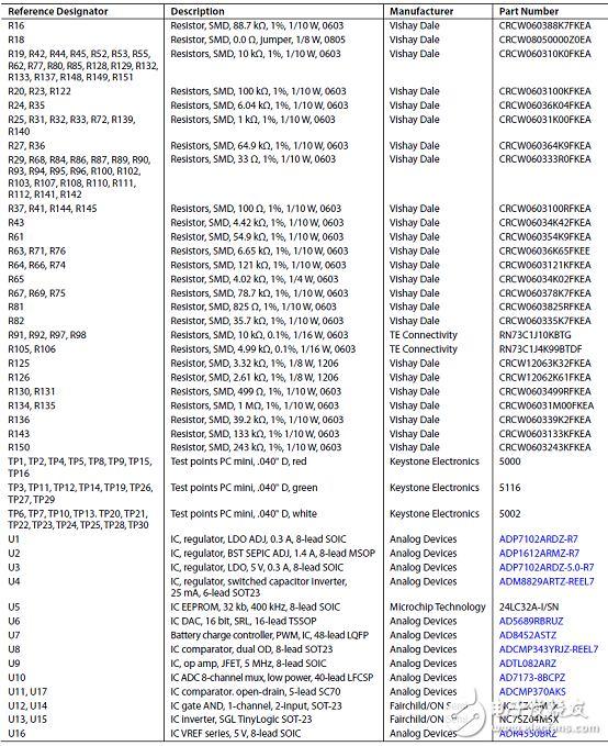
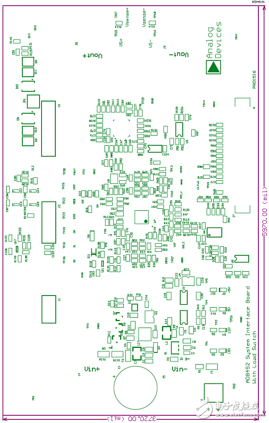
图26.模拟接口板PCB设计图(1):丝印图
图27.模拟接口板PCB设计图(2):顶层布局图
图28.模拟接口板PCB设计图(3):层2
图29.模拟接口板PCB设计图(4):层3
图30.模拟接口板PCB设计图(5):底层

图31.模拟接口板PCB设计图(6):底层丝印
图32.模拟接口板PCB设计图(7):综合图
-
AD8452:电池测试与形成系统的理想之选2026-01-14 326
-
AD8452-EVALZ AD8452 评估板2021-05-29 765
-
UG-1180:AD8452通用评估板2021-04-23 642
-
UG-1181:AD8452系统演示评估板2021-04-22 751
-
AD8452演示电路-充电模式(4.2V 10A)2021-04-09 1069
-
AD8452 Demo Circuit - Charging Mode (4.2V 10A)2021-02-03 754
-
基于AD8452单硅芯片的电池化成控制系统综合解决方案2020-10-27 1300
-
NCP51705主要特性_内部框图以及应用电路2019-05-11 5995
-
MAX40056主要特性以及应用电路2019-04-05 6501
-
AD8452 用于电池测试和化成系统的精密集成模拟前端、控制器和 PWM2019-02-22 2018
-
LT8607的主要特性,功能框图,多种应用电路解析2018-02-11 2418
全部0条评论

快来发表一下你的评论吧 !
