

FS4503混合和动力汽车系统基础芯片(SBS)解决方案
汽车电子
描述
nxp公司的FS4503具有CAN灵活数据收发器的Grade 1和Grade 0安全功率系统基础芯片(SBS),通过DC/DC预稳压和线性稳压器以及超低功耗节电模式来给MCU供电和优化能量损耗,最大输入电压36V,主要用在驱动列车电气化(BMS,混合EV和HEV,逆变器,DCDC),驱车列车底盘和安全(主动悬挂,转向装置,安全域网关),动力传动系(EMS,TCU,变速箱以及ADAS(LDW,雷达,传感器融合安全区)等。本文介绍了FS4503主要特性,框图和应用电路,以及评估板KITFS6522LAEEVM, KITFS6523CAEEVM和KITFS4503CAEEVM主要特性,框图,电路图,材料清单和PCB装配图。
The NXP® FS4500 system basis chip (SBC) provides power to MCUs and optimizes energy consumption through a DC/DC pre-regulator and linear regulators and ultra-low-power saving modes.
The FS6500/FS4500 SMARTMOS devices are a multi-output, power supply,integrated circuit, including CAN Flexible Data (FD) and/or LIN transceivers, dedicated to the automotive market.
Multiple switching and linear voltage regulators, including low-power mode (32 μA) are available with various wake-up capabilities. An advanced power management scheme is implemented to maintain high efficiency over a wide range of input voltages (down to 2.7 V) and output current ranges (up to 2.2 A)。
The FS6500/FS4500 includes configurable fail-safe/fail silent safety behavior and features, with two fail-safe outputs, becoming a full part of a safety oriented system partitioning, to reach a high integrity safety level (up to ASIL D)。
The built-in CAN FD interface fulfills the ISO 11898-2 and -5 standards. The LIN interface fulfills LIN protocol specifications 2.0, 2.1, 2.2, and SAEJ2602-2.
FS4503主要特性:
• Battery voltage sensing and MUX output pin
• Highly flexible SMPS pre-regulator, allowing two topologies: non-inverting buck-boost and standard buck
• Family of devices to supply MCU core from 1.0 V to 5.0 V, with SMPS (0.8 A, 1.5 A or 2.2 A) or LDO (0.5 A)
• 36 V maximum input operating voltage
• Linear voltage regulator dedicated to auxiliary functions, or to sensor supply (VCCA tracker or independent), 5.0 V or 3.3 V
• Linear voltage regulator dedicated to MCU A/D reference voltage or I/Os supply (VCCA),5.0 V or 3.3 V
• 3.3 V keep alive memory supply available in low-power mode
• Long duration timer, counting up to 6 months with 1.0 s resolution
• Multiple wake-up sources in low-power mode: CAN, LIN, IOs, LDT
• Five configurable I/Os
FS4503应用:
• Drive train electrification (BMS, hybrid EV and HEV, inverter, DCDC, alterno starter)
• Drive train - chassis and safety (active suspension, steering, safety domain gateway)
• Power train (EMS, TCU, gear box)
• ADAS (LDW, Radar, sensor fusion safety area)
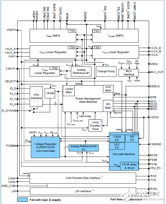
图1.具有CAN 和LIN的FS6500/FS4500简化框图
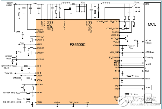
图2.FS6500C简化应用电路-降压-升压配置-FS1B
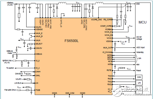
图3.FS6500L简化应用电路-降压配置-LIN-VccA=100mA
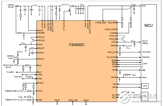
图4.FS4500C简化应用电路-降压-升压配置-FS1B
评估板KITFS6522LAEEVM, KITFS6523CAEEVM和KITFS4503CAEEVM
The KITFS6522LAEEVM, KITFS6523CAEEVM, and KITFS4503CAEEVM are hardware evaluation tools supporting system designs based on NXP’s FS4500 and FS6500 product families. The kits allow testing the devices as an integral part of the overall system being developed. They provide access to all FS45xx and FS65xx functions (SPI, IOs) and support functional modes such as debug, normal, buck, and boost.
评估板KITFS6522LAEEVM, KITFS6523CAEEVM和KITFS4503CAEEVM主要特性:
•VBAT power supply either through power jack (2.0 mm) or phoenix connector
•VCORE configuration:1.23 V, 3.3 V, and 5.0 V
•VCCA configuration:
–3.3 V or 5.0 V
–Internal transistor or external PNP
•VAUX configuration: 3.3 V or 5.0 V
•Buck or boost setting
•DFS configuration
•Ignition key switch
•LIN bus (optional)
•CAN bus
•FS0B
•FS1B (Option)
•IO connector (IO_0 to IO_5)
•Debug connector (SPI bus, CAN digital, LIN digital, RSTB, FS0B, INTB, Debug, MUX_OUT)
•Signalling LED to give state of signals or regulators
•KL25Z MCU installed on board for easy connection to host computer on USB link
图5.评估板FS45xx/FS65xx外形图
The KITFS6522LAEEVM, KITFS6523CAEEVM, and KITFS4503CAEEVM kit contents include:
•Assembled and tested evaluation boards/modules in anti-static bag
•Connector, terminal block plug, 2 pos., str. 3.81 mm
•Connector, terminal block plug, 10 pos., str. 3.81 mm
•Cable, assy, USB-STD A to USB-B-mini 3.0 ft.
•Quick start guide
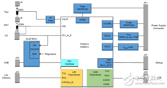
图6.评估板FS45xx/FS65xx框图
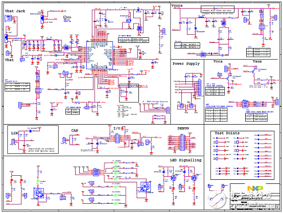
图7.评估板FS45xx/FS65xx电路图(1)
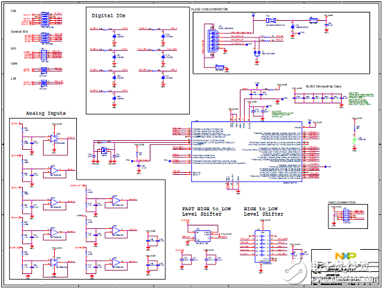
图8.评估板FS45xx/FS65xx电路图(2)
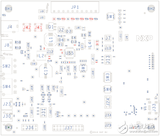
图9.评估板FS45xx/FS65xx PCB设计图(1):顶层装配图
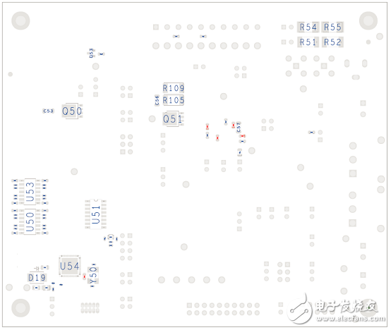
图10.评估板FS45xx/FS65xx PCB设计图(2):底层装配图
评估板FS45xx/FS65xx材料清单见:
KITFS4503CAEEVM_BOM_Report.xls
详情请见:
https://www.nxp.com/docs/en/product-numbering-scheme/FS6500-FS4500SDS.pdf
和https://www.nxp.com/docs/en/user-guide/KTFS4500-FS6500UG.pdf
FS6500-FS4500SDS.pdf
KTFS4500-FS6500UG.pdf
-
为混合动力汽车/电动汽车设计暖通系统的教程2022-11-07 1977
-
高性能集成动力总成的解决方案2022-11-04 1097
-
混合动力汽车2022-05-10 4603
-
混合动力汽车电动汽车中高压电流感应的挑战及解决办法2020-10-30 2149
-
英飞凌汽车电子解决方案2018-12-13 6347
-
混合动力汽车改变了什么2018-10-11 2102
-
汽车电池管理系统和混合动力BMS2018-07-25 4078
-
汽车混合动力传动系统解决方案2016-01-06 581
-
汽车动力系统大盘点:助你设计绝佳方案2015-04-21 4625
-
汽车动力系统解决方案集锦2015-04-20 4632
-
面向新兴微混合动力应用的先进电力电子解决方案2012-12-20 2507
-
混合动力汽车电子差速控制系统的研究2009-05-17 3398
全部0条评论

快来发表一下你的评论吧 !

