

ADP1071-1/ADP1071-2隔离功能反激控制器解决方案
控制/MCU
描述
ADI公司的ADP1071-1/ADP1071-2是集成了隔离功能和SR驱动器及轻负载模式的反激式控制器,消除了变压器和光耦合器件,降低了系统设计复杂性,成本和元件数量,并提高了系统可靠性。器件集成了误差放大器和优于1%精度基准电压,可编程开关频率50 kHz - 600 kHz,主要用在隔离的DC/DC和AC/DC转换器,通信和工业,小型基站,PoE供电设备,企业交换器和路由器。本文介绍了ADP1071-1/ADP1071-2主要特性,框图,应用电路图以及评估板ADP1071-1EVALZ和评估板ADP1071-2EBZ3.3V主要特性,电路图,材料清单和PCB设计图。
The ADP1071-1/ADP1071-2 are pulse-width modulation (PWM) current mode fixed frequency synchronous flyback controllers designed for isolated dc-to-dc power supplies. Analog Devices proprietary iCouplers® are integrated in the ADP1071-1/ADP1071-2 to eliminate the bulky signal trans-formers and optocouplers that transmit signals over the isolation boundary. Integrating the iCouplers reduces system design complexity, cost, and component count and improves overall system reliability. With the integrated isolators and metal-oxide semiconductor field effect transistor (MOSFET) drivers on both the primary and the secondary side, the ADP1071-1/ADP1071-2 offer a compact system level design and yield a higher efficiency than a diode rectified flyback converter at heavy loads.
Output regulation is achieved by sensing the output voltage on the secondary side, where the feedback and the PWM signals are transmitted between the primary and secondary sides through the iCouplers.
The ADP1071-1/ADP1071-2 are offered in a 16-lead SOIC_W package with an isolation voltage rating of 5 kV rms. The ADP1071-2 is designed for isolated dc-to-dc applications typically with an input voltage less than 36 V, and the ADP1071-1 targets high input voltage applications, in which the dc input voltage can exceed 60 V.
The ADP1071-1/ADP1071-2 offer features such as input current protection, output overvoltage protection (OVP), undervoltage lockout (UVLO), precision enable with adjustable hysteresis, overtemperature protection (OTP), and power saving light load mode (LLM)。
ADP1071-1/ADP1071-2主要特性:
Current mode controller for flyback topology
ADP1071-1: programmable LLM or CCM for high VIN applications
ADP1071-2: forced CCM operation
Programmable slope compensation
Integrated 5 kV isolation with Analog Devices, Inc., iCoupler technology
Wide voltage supply range
Primary VDD: up to 60 V (ADP1071-2 only)
Secondary VDD2: up to 36 V
Integrated 1 A primary side MOSFET driver
Integrated 1 A secondary side MOSFET drivers for synchronous rectification
Integrated error amplifier and 《1% accurate reference voltage
Programmable frequency range: 50 kHz to 600 kHz
Duty cycle clamp limit 85%
Programmable soft start and soft start from precharged load
Protection features such as short circuit, output overvoltage, and overtemperature protection
Power saving LLM using MODE pin (ADP1071-1only)
Cycle by cycle input overcurrent protection
Precision enable UVLO with hysteresis
Frequency synchronization
Safety and regulatory approvals (pending)
UL recognition
5000 V rms for 1 minute per UL 1577
CSA Component Acceptance Notice 5A
VDE certificate of conformity
DIN V VDE V 0884-10 (VDE V 0884-10):2006-12
VIORM = 849 V peak
CQC certification per GB4943.1-2011
Available in 16-lead SOIC_W package
ADP1071-1/ADP1071-2应用:
Isolated dc-to-dc or ac-to-dc power conversion
Telecom, industrial
Small cell
PoE powered device
Enterprise switches and routers
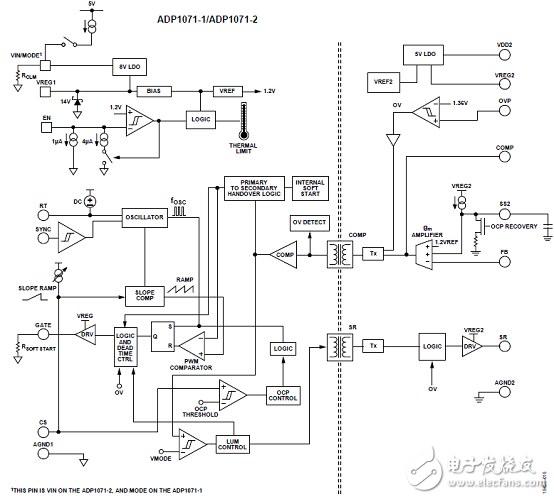
图1.ADP1071-1/ADP1071-2框图
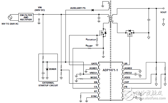
图2.ADP1071-1/ADP1071-2外接起动电路和辅助电源的应用电路
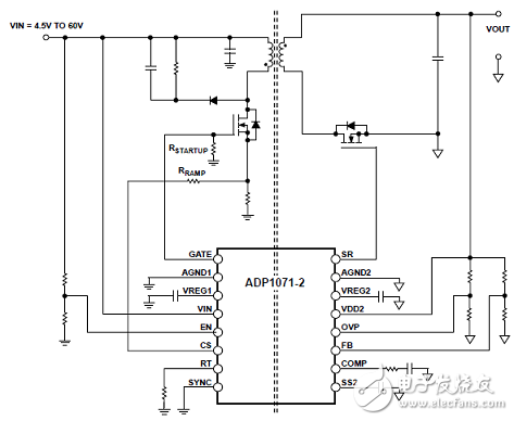
图3.ADP1071-1/ADP1071-2低输入电压反激应用电路图
评估板ADP1071-1EVALZ
The ADP1071-1EVALZ allows users to evaluate the ADP1071-1 in flyback topology. The evaluation board is set up to act as an isolated power supply solution that incorporates three output voltages (+5.5 V, +24 V, and −15 V) at a total rated power of 15 W. The evaluation board also provides 5 kV isolation in compact form factor, making it suitable for industrial applications, which usually have a variety of voltage rails.
Complete information about the ADP1071-1 is available in the ADP1071-1/ADP1071-2 data sheet. Consult the ADP1071-1/ ADP1071-2 data sheet in conjunction with this user guide when using the evaluation board.
评估板ADP1071-1EVALZ主要特性:
Full support evaluation kit for the ADP1071-1
15 W multioutput flyback topology
+24 V, +5.5 V, and −15 V output voltage (VDC)
Light load mode (LLM) operation
Dedicated internal primary and secondary side MOSFET drivers
External reference signal tracking
Precision enabled undervoltage lockout with hysteresis
Short-circuit, output overvoltage, cycle by cycle input overcurrent, and overtemperature protection
Frequency synchronization
Soft start and soft stop functionality
图4.评估板ADP1071-1EVALZ数字外形图(正面)
图5.评估板ADP1071-1EVALZ数字外形图(背面)
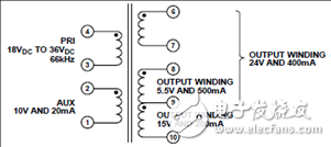
图6.变压器电路图
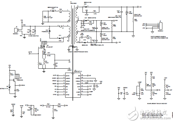
图7.评估板ADP1071-1EVALZ电路图
评估板ADP1071-1EVALZ材料清单:
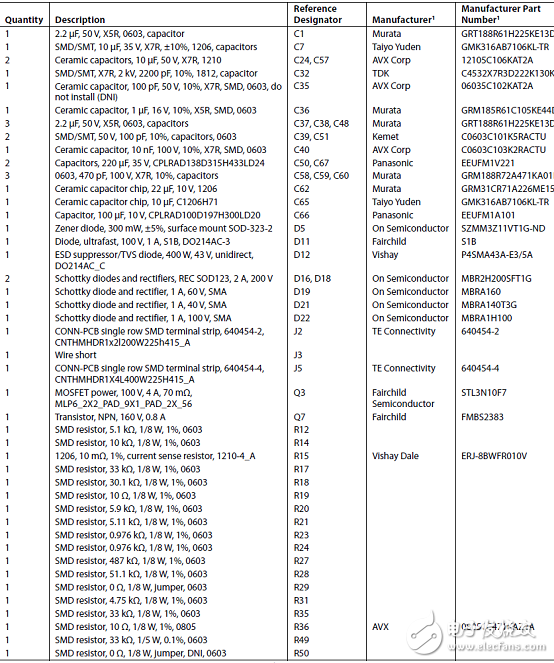
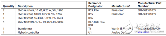
图8.评估板ADP1071-1EVALZ PCB设计图(1):左:板尺寸;右:底层丝印
图9.评估板ADP1071-1EVALZ PCB设计图(2):左:顶层丝印;右:顶层布局
图10.评估板ADP1071-1EVALZ PCB设计图(3):左:层2;右:层4
图11.评估板ADP1071-1EVALZ PCB设计图(4):层3
评估板ADP1071-2EBZ3.3V
The ADP1071-2EBZ3.3V evaluation board allows users to evaluate the ADP1071-2 in a power supply application.
The ADP1071-2EBZ3.3V evaluation board is set up to act as an isolated power supply unit (PSU), with a rated load of 3.3 Vdc 3 A from a 36 Vdc to 60 Vdc source. There is also an auxiliary output of 8.0 Vdc, 10 mA. The operation of the converter is in continuous conduction mode (CCM)。
All connectors and multiple test points allow easy access to all critical circuit nodes and pins of the ADP1071-2.
Multiple test points allow easy access to all critical circuit nodes and pins of the ADP1071-2.
Full data on the ADP1071-2 can be found in the ADP1071-2 data sheet, available from Analog Devices, Inc., which must be consulted in conjunction with this user guide when using the evaluation board.
评估板ADP1071-2EBZ3.3V主要特性:
Full support evaluation kit for the ADP1071-2
10 W flyback topology
3.3 V output voltage (Vdc)
3 A steady state
Auxiliary output of 8.0 Vdc, 10 mA
Forced CCM operation
Integrated drivers primary side MOSFET and secondary side synchronous rectifier
External reference signal tracking
Precision enable undervoltage lockout with hysteresis
Short-circuit, output overvoltage, and overtemperature protection
Cycle by cycle input overcurrent protection
Frequency synchronization
Soft start and soft stop functionality
图12.评估板ADP1071-2EBZ3.3V外形图
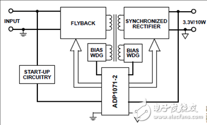
图13.评估板ADP1071-2EBZ3.3V框图
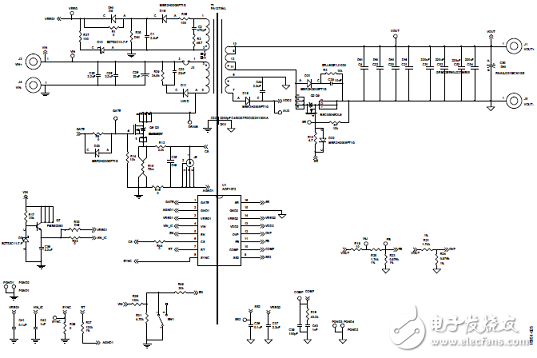
图14.评估板ADP1071-2EBZ3.3V电路图
评估板ADP1071-2EBZ3.3V材料清单:
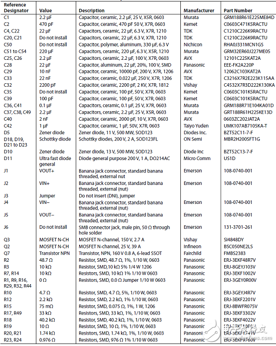
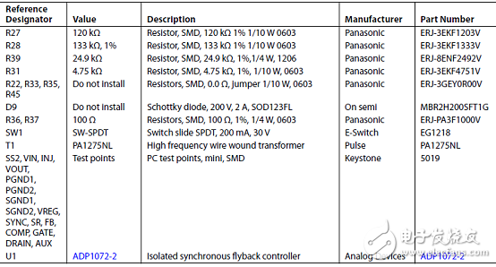
图15.评估板ADP1071-2EBZ3.3V PCB设计图(1):顶层丝印
图16.评估板ADP1071-2EBZ3.3V PCB设计图(2):底层丝印
图17.评估板ADP1071-2EBZ3.3V PCB设计图(3):顶层布局
图18.评估板ADP1071-2EBZ3.3V PCB设计图(4):层2
图19.评估板ADP1071-2EBZ3.3V PCB设计图(5):层3
图20.评估板ADP1071-2EBZ3.3V PCB设计图(6):层4
详情请见:
和
以及
ADP1071-1-1071-2.pdf
ADP1071-1EVALZ-UG-1384.pdf
ADP1071-2EBZ3.3V.pdf
- 相关推荐
- 热点推荐
- �
-
ADP1074:隔离式同步正激控制器的卓越之选2026-03-06 370
-
ADP1074/ADP1071-1/ADP1071-2的电源故障排除2023-11-28 575
-
EVAL-ADP1071-2 EVAL-ADP1071-2评估板2021-07-14 216
-
基于ADP1071-1EVALZ直流到直流多输出电源的参考设计2021-07-04 602
-
ADP1613隔离式反激转换器;输入+30-2021-05-27 888
-
ADP1071-1/ADP1071-2:集成<span class=“模拟耦合器”>i</span>耦合器数据表的隔离式同步反激控制器2021-05-13 1038
-
ADP1071-1EVALZ用户指南2021-05-08 748
-
ADP1071-2 集成了隔离功能和SR驱动器的反激式控制器2019-02-22 374
-
使用我们的icoupler技术、全面集成闭环反馈路径的全新系列隔离式DC/DC控制器介绍2018-06-01 4855
-
ADI公司推出集成式隔离电源控制器系列2017-03-27 1905
全部0条评论

快来发表一下你的评论吧 !
