

基于Cypress PSoC 63 MCU系列开发方案
电子说
描述
Cypress公司的PSoC 63 MCU系列是集成了Arm® Cortex™ CPU(单核和多核)的可升级和可配置的可编嵌入系统控制器,采用超低功耗40nm平台,包括有低功耗闪存和数字可编逻辑的双核微控制器(150-MHz Arm Cortex-M4F CPU和100-MHz Cortex M0+ CPU),高性能模数和数模转换器,低功耗比较器以及标准通信和定时外设,并提供BLE 5.0兼容的无线连接,可开发各种创新型物联网应用.主要用在可穿戴设备,个人医疗设备和无线音箱等.本文介绍了PSoC 63 MCU系列主要特性,框图,以及评估板CY8CKIT-062-BLE主要特性,框图和电路图.
PSoC® is a scalable and reconfigurable platform architecture for a family of
programmable embedded system controllers with Arm® Cortex™ CPUs (single and multi-core). The PSoC 63 product family, based on an ultra low-power 40-nm platform, is a combination of a dual-core microcontroller with low-power Flash technology and digital programmable logic, high-performance analog-to-digital and digital-to-analog conversion, low-power comparators, and standard communication and timing peripherals. The PSoC 63 family provides wireless connectivity with BLE 5.0 compliance.
PSoC 63 MCU系列主要特性:
32-bit Dual Core CPU Subsystem
■ 150-MHz Arm Cortex-M4F CPU with single-cycle multiply (Floating Point and Memory Protection Unit)
■ 100-MHz Cortex M0+ CPU with single-cycle multiply and MPU.
■ User-selectable core logic operation at either 1.1 V or 0.9 V
■ Inter-processor communication supported in hardware
■ 8 KB 4-way set-associative Instruction Caches for the M4 and M0+ CPUs respectively
■ Active CPU power consumption slope with 1.1-V core operation for the Cortex M4 is 40 μA/MHz and 20 μA/MHz for the Cortex M0+, both at 3.3-V chip supply voltage with the internal buck regulator
■ Active CPU power consumption slope with 0.9-V core operation for the Cortex M4 is 22 μA/MHz and 15 μA/MHz for the Cortex M0+, both at 3.3-V chip supply voltage with the internal buck regulator
■ Two DMA controllers with 16 channels each
Flash Memory Sub-system
■ 1 MB Application Flash with 32-KB EEPROM area and 32-KB Secure Flash
■ 128-bit wide Flash accesses reduce power
■ SRAM with Selectable Retention Granularity
■ 288-KB integrated SRAM
■ 32-KB retention boundaries (can retain 32 KB to 288 KB in 32-KB increments)
■ One-Time-Programmable (OTP) E-Fuse memory for validation and security
Bluetooth Low Energy (Bluetooth Smart) BT 5.0 Subsystem
■ 2.4-GHz RF transceiver with 50-ohm antenna drive
■ Digital PHY
■ Link Layer engine supporting master and slave modes
■ Programmable output power: up to 4 dBm
■ RX sensitivity: –95 dBm
■ RSSI: 4-dB resolution
■ 5.7 mA TX (0 dBm) and 6.7 mA RX (2 Mbps) current with 3.3-V battery and internal SIMO Buck converter
■ Link Layer engine supports four connections simultaneously
■ Supports 2 Mbps LE data rate
Low-Power 1.7-V to 3.6-V Operation
■ Active, Low-power Active, Sleep, Low-power Sleep, Deep Sleep, and Hibernate modes for fine-grained power management
■ Deep Sleep mode current with 64-KB SRAM retention is 7 μA with 3.3-V external supply and internal buck
■ On-chip Single-In Multiple Out (SIMO) DC-DC Buck converter, <1 μA quiescent current
■ Backup domain with 64 bytes of memory and Real-Time-Clock
Flexible Clocking Options
■ On-chip crystal oscillators (High-speed, 4 to 33 MHz, and Watch crystal, 32 kHz)
■ Phase Locked Loop (PLL) for multiplying clock frequencies
■ 8 MHz Internal Main Oscillator (IMO) with ±2% accuracy
■ Ultra low-power 32 kHz Internal Low-speed Oscillator (ILO) with ±10% accuracy
■ frequency Locked Loop (FLL) for multiplying IMO frequency
Serial Communication
■ Nine independent run-time reconfigurable serial communication blocks (SCBs), each is software configurable as I2C, SPI, or UART
Timing and Pulse-Width Modulation
■ Thirty-two Timer/Counter Pulse-Width Modulator (TCPWM) blocks
■ Center-aligned, Edge, and Pseudo-random modes
■ Comparator-based triggering of Kill signals
Up to 78 Programmable GPIOs
■ Drive modes, strengths, and slew rates are programmable
■ Six overvoltage tolerant (OVT) pins
Packages
■ 116-BGA and 104-MCSP packages with PSoC 6 and BLE Radio
Audio Subsystem
■ I2S Interface; up to 192 kilosamples (ksps) Word Clock
■ Two PDM channels for stereo digital microphones
QSPI Interface
■ Execute-In-Place (XIP) from external Quad SPI Flash
■ On-the-fly encryption and decryption
■ 4-KB QSPI cache for greater XIP performance with lower power
■ Supports 1, 2, 4, and Dual-Quad interfaces
Programmable Analog
■ 12-bit 1 Msps SAR ADC with differential and single-ended modes and Sequencer with signal averaging
■ One 12-bit voltage mode DAC with < 5-μs settling time
■ Two opamps with low-power operation modes
■ Two low-power comparators that operate in Deep Sleep and Hibernate modes.
■ Built-in temp sensor connected to ADC
Programmable Digital
■ 12 programmable logic blocks, each with 8 Macrocells and an 8-bit data path (called universal digital blocks or UDBs)
■ Usable as drag-and-drop Boolean primitives (gates, registers), or as Verilog programmable blocks
■ Cypress-provided peripheral component library using UDBs to implement functions such as Communication peripherals (for example, LIN, UART, SPI, I2C, S/PDIF and other protocols), Waveform Generators, Pseudo-Random Sequence (PRS) generation, and many other functions.
■ Smart I/O (Programmable I/O) blocks enable Boolean operations on signals coming from, and going to, GPIO pins
■ Two ports with Smart_IO blocks, capability are provided; these are available during Deep Sleep
Capacitive Sensing
■ Cypress Capacitive Sigma-Delta (CSD) provides best-in-class SNR, liquid tolerance, and proximity sensing
■ Mutual Capacitance sensing (Cypress CSX) with dynamic usage of both Self and utual sensing
■ Wake on Touch with very low current
■ Cypress-supplied software component makes capacitive sensing design fast and easy
■ Automatic hardware tuning (SmartSense™)
Energy Profiler
■ Block that provides history of time spent in different power modes
■ Allows software energy profiling to observe and optimize energy consumption
PSoC Creator Design Environment
■ Integrated Development Environment provides schematic design entry and build (with analog and digital automatic routing) and code development and debugging
■ Applications Programming Interface (API Component) for all fixed-function and programmable peripherals
■ Bluetooth Smart Component (BLE4.2 compliant protocol stack) with Application level function calls and Profiles
Industry-Standard Tool Compatibility
■ After schematic entry, development can be done with Arm-based industry-standard development tools
■ Configure in PSoC Creator and export to Arm/Keil or IAR IDEs for code development and debugging
■ Supports industry standard Arm Trace Emulation Trace Module
Security Built into Platform Architecture
■ Multi-faceted secure architecture based on ROM-based root of trust
■ Secure Boot uninterruptible until system protection attributes are established
■ Authentication during boot using hardware hashing
■ Step-wise authentication of execution images
■ Secure execution of code in execute-only mode for protected routines
■ All Debug and Test ingress paths can be disabled
Cryptography Accelerators
■ Hardware acceleration for Symmetric and Asymmetric cryptographic methods (AES, 3DES, RSA, and ECC) and Hash functions (SHA-512, SHA-256)
■ True Random Number Generator (TRNG) function

图1. PSoC 63 MCU系列框图
评估板CY8CKIT-062-BLE
Thank you for your interest in the CY8CKIT-062-BLE PSoC 6 BLE Pioneer Kit. The PSoC 6 BLE Pioneer Kit enables you to evaluate and develop your applications using the PSoC 6 MCU with Bluetooth Low Energy (BLE) Connectivity (hereafter called “PSoC 6 MCU”).
PSoC 6 MCU is Cypress’ latest, ultra-low-power PSoC specifically designed for wearables and IoT products. PSoC 6 MCU is a true programmable embedded system-on-chip, integrating a 150-MHz ARM® Cortex®-M4 as the primary application processor, a 100-MHz ARM Cortex®-M0+ that supports low-power operations, up to 1 MB Flash and 288 KB SRAM, an integrated BLE 4.2 radio, CapSense® touch-sensing, and programmable analog and digital peripherals that allow higher flexibility, in-field tuning of the design, and faster time-to-market.
The PSoC 6 BLE Pioneer board offers compatibility with Arduino™ shields. The board features a PSoC 6 MCU, a 512-Mb NOR flash, onboard programmer/debugger (KitProg2), USB Type-C power delivery system (EZ-PD™ CCG3), 5-segment CapSense slider, two CapSense buttons, one Cap-Sense proximity sensing header, an RGB LED, two user LEDs, and one push button. The board supports operating voltages from 1.8 V to 3.3 V for PSoC 6 MCU.
The CY8CKIT-062-BLE package includes a CY8CKIT-028-EPD E-INK Display Shield that contains a 2.7-inch E-INK display, a motion sensor, a thermistor, and a PDM microphone. The kit package also contains a CY5677 CySmart BLE 4.2 USB Dongle that is factory-programmed to emulate a BLE GAP Central device, enabling you to emulate a BLE host on your computer.
You can use PSoC Creator™ to develop and debug your PSoC 6 MCU projects. PSoC Creator is Cypress’ standard integrated design environment (IDE). PSoC Creator also supports exporting your designs to other third party firmware development tools.
If you are new to PSoC 6 MCU and PSoC Creator IDE, you can find introductions in the application note AN210781 - Getting Started with PSoC 6 MCU with Bluetooth Low Energy (BLE) Connectivity.
The CY8CKIT-062-BLE package has the following contents.
■ PSoC 6 BLE Pioneer Board
■ CY8CKIT-028-EPD E-INK Display Shield
■ CY5677 CySmart BLE 4.2 USB Dongle
■ USB Type-A to Type-C cable
■ Four jumper wires (4 inches each)
■ Two proximity sensor wires (5 inches each)
■ Quick Start Guide
图2. 评估板CY8CKIT-062-BLE组图外形图
评估板CY8CKIT-062-BLE主要特性:
■ PSoC 6 MCU with BLE connectivity
■ Expansion headers that are compatible with Arduino Uno™ 3.3 V shields1 and Digilent® Pmod™ modules
■ 512-Mbit external quad-SPI NOR Flash that provides a fast, expandable memory for data and code
■ KitProg2 onboard programmer/debugger with mass storage programming, USB to UART/I2C/ SPI bridge functionality, and custom applications support
■ EZ-PD CCG3 USB Type-C power delivery (PD) system with rechargeable lithium-ion polymer (Li-Po) battery support2
■ CapSense touch-sensing slider (5 elements), two buttons, all of which are capable of both selfcapacitance (CSD) and mutual-capacitance (CSX) operation, and a CSD proximity sensor that let you evaluate Cypress’ fourth-generation CapSense technology
■ 1.8 V to 3.3 V operation of PSoC 6 MCU is supported. An additional 330 mF super-capacitor is provided for backup domain supply (Vbackup)
■ Two user LEDs, a RGB LED, a user button, and a reset button for PSoC 6 MCU. Two buttons and three LEDs for KitProg2
图3. 评估板PSoC 6 BLE Pioneer板外形图(正面)
评估板PSoC 6 BLE Pioneer板中数字内容为:
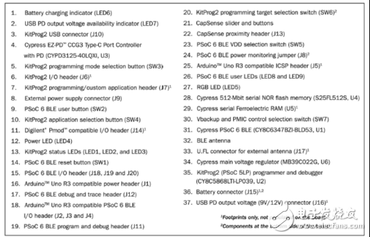
图4. 评估板PSoC 6 BLE Pioneer板框图
图5. 评估板PSoC 6 BLE Pioneer板电路图(1)

图6. 评估板PSoC 6 BLE Pioneer板电路图(2)

图7. 评估板PSoC 6 BLE Pioneer板电路图(3)

图8. 评估板PSoC 6 BLE Pioneer板电路图(4)

图9. 评估板PSoC 6 BLE Pioneer板电路图(5)

图10. 评估板PSoC 6 BLE Pioneer板电路图(6)

图11. 评估板PSoC 6 BLE Pioneer板电路图(7)

图12. 评估板PSoC 6 BLE Pioneer板电路图(8)

图13. 评估板PSoC 6 BLE Pioneer板电路图(9)

图14. 评估板PSoC 6 BLE Pioneer板电路图(10)
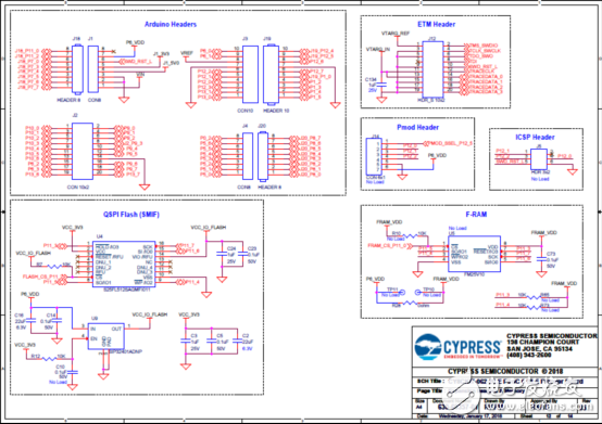
图15. 评估板PSoC 6 BLE Pioneer板电路图(11)

图16. 评估板PSoC 6 BLE Pioneer板电路图(12)
-
CYPRESS 集成开发环境(IDE)WICED Studio的使用2021-11-13 1492
-
赛普拉斯Cypress PSoC 6 MCU简介及常见4款开发套件工具板2019-12-10 18500
-
Cypress PSoC®5开发板特性_电路图及PCB元件布局图2019-07-13 2074
-
Cypress TrueTouch电容触摸屏的通讯接口设计方案2019-01-28 4363
-
cypress公司的PSoC 4000Pioneer开发板方案介绍2018-05-05 3374
-
e络盟推出 Cypress PSoC 6 BLE 先锋套件:开发提供高性能、低功耗且可实现最大安全性的下一代物联网设计2017-12-19 10764
-
Cypress的PSoC系列产品CY8C22x45_CY8C21345数据手册免费下载2017-10-10 2057
-
深入测试:大道至简—Cypress PSoC 4000S CapSense原型开发套件评测(二)2017-09-20 9699
-
PSoC 6横空出世,奠定Cypress在IOT市场领先地位2017-04-10 4986
-
cypress的PSoC的开发板有多少种类型?在哪里可以买到cypress的PSoC的开发板?2015-10-15 4642
-
Cypress PSoC蓝牙低功耗开发设计攻略2015-05-08 4498
-
Cypress PSoC蓝牙低功耗开发方案与电路图详解2015-04-29 9909
-
Mouser备货Cypress PSoC 4可编程SoC2013-06-13 1431
-
PSoC Creator IDE的编译器是cypress与K2010-03-04 1689
全部0条评论

快来发表一下你的评论吧 !
