
可升级和可配置的PSoC62系列MCU平台架构
控制/MCU
描述
Cypress公司的PSoC 62系列MCU是可升级和可配置的平台架构,采用超低功耗40nm技术,组合了双核MCU(150-MHz Arm Cortex-M4F CPU和100-MHz Cortex M0+ CPU)和低功耗闪存(多达2MB)以及1MB SRAM,数字可编逻辑,高性能模数和数模转换器,低功耗比较器以及其标准通信和定时外设。器件可提供多达104 GPIO,工作电压1.7V-3.6V,主要用在可爱穿戴,智能家居,工业IoT,手持医疗设备等。本文介绍了PSoC 62系列主要特性,框图和时钟框图,以及PSoC 6 Wi-Fi BT原型套件CY8CPROTO-062-4343W主要特性,电路图,材料清单和PCB设计图与装配图。
PSoC® is a scalable and reconfigurable platform architecture for a family of programmable embedded system controllers with Arm®Cortex™ CPUs (single and multi-core)。 The PSoC 6 product family, based on an ultra low-power 40-nm platform, is a combination ofa dual-core microcontroller with low-power Flash technology and digital programmable logic, high-performance analog-to-digital anddigital-to-analog conversion, low-power comparators, and standard communication and timing peripherals.
PSoC 62系列主要特性:
32-bit Dual Core CPU Subsystem
■ 150-MHz Arm Cortex-M4F CPU with single-cycle multiply(Floating Point and Memory Protection Unit)
■ 100-MHz Cortex M0+ CPU with single-cycle multiply and MPU
■ User-selectable core logic operation at either 1.1 V or 0.9 V
■ Inter-processor communication supported in hardware
■ 8 KB 4-way set-associative Instruction Caches for the M4 andM0+ CPUs respectively
■ Active CPU power consumption slope with 1.1 V core operationfor the Cortex M4 is 40 μA/MHz and 20 μA/MHz for the CortexM0+, both at 3.3 V chip supply voltage with the internal buckregulator
■ Active CPU power consumption slope with 0.9 V core operationfor the Cortex M4 is 22 μA/MHz and 15 μA/MHz for the CortexM0+, both at 3.3 V chip supply voltage with the internal buckregulator
■ Three DMA controllers
Flexible Memory Sub-system
■ 2 MB Application Flash with 32 KB EEPROM area and 32 KBSupervisory Flash
■ 128-bit wide Flash accesses reduce power
■ Flash Read-While-Write (RWW) allows updating the Flashwhile executing from it
■ SRAM with Selectable Retention Granularity
■ 1024 KB SRAM (three independent blocks of 512 KB, 256 KB,and 256 KB)
■ 32 KB retention boundaries (in the 512 KB block)
■ One-Time-Programmable (OTP) E-Fuse memory for validationand security
Low-Power 1.7-V to 3.6-V Operation
■ Active, Low-power Active, Sleep, Low-power Sleep, DeepSleep, and Hibernate modes for fine-grained powermanagement
■ Deep Sleep mode current with 64K SRAM retention is 7 μAwith 3.3 V external supply and internal buck
■ On-chip DC-DC Buck converter, 《1 μA quiescent current
■ Backup domain with 64 bytes of memory and Real-time Clock(RTC)
Flexible Clocking Options
■ On-chip crystal oscillators (High-speed, 4 to 33 MHz, andWatch crystal, 32 kHz)
■ Two Phase-locked Loops (PLLs) for multiplying clockfrequencies
■ 8 MHz Internal Main Oscillator (IMO) with 2% accuracy
■ Ultra low-power 32 kHz Internal Low-speed Oscillator (ILO)with 10% accuracy
■ frequency Locked Loop (FLL) for multiplying IMO frequency
Serial Communication
■ 13 independent run-time reconfigurable serial communicationblocks (SCBs), eight are software-configurable as SPI, I2C, orUARTs. One SCB can operate in Deep Sleep with an externalclock and can be either SPI or I2C. The other four can be eitherUARTs or I2C.
■ USB Full-Speed Dual-role Host and Device interface
Timing and Pulse-Width Modulation
■ Thirty-two Timer/Counter Pulse-Width Modulator (TCPWM)blocks
■ Center-aligned, Edge, and Pseudo-random modes
■ Comparator-based triggering of Kill signals
Up to 104 Programmable GPIOs
■ Drive modes, strengths, and slew rates are programmable
■ Six overvoltage tolerant (OVT) pins
Packages
■ 124-BGA
■ 128 TQFP
■ 100 WLCSP
Audio Subsystem
■ Two I2S Interfaces; up to 192 kilosamples Word Clock
■ Two PDM channels for stereo digital microphones
QSPI Interface
■ Execute-In-Place (XIP) from external Quad SPI Flash
■ On-the-fly encryption and decryption
■ 4 KB QSPI cache for greater XIP performance with lower power
■ Supports 1, 2, 4, and Dual-Quad interfaces
Secure Digital Host Controller (SDHC) with eMMC
■ Two independent SDHC/eMMC/SD controllers
■ Operation up to 80 MHz (SDR-50) supported
■ Provide connectivity to IoT Wireless devices
Programmable Analog
■ 12-bit 1 Msps SAR ADC with differential and single-endedmodes and 16-Channel Sequencer with signal averaging
■ Two low-power comparators that operate in Deep Sleep andHibernate modes.
■ Built-in temp sensor connected to ADC
Programmable Digital
■ Smart I/O (Programmable I/O) blocks enable Booleanoperations on signals coming from, and going to, GPIO pins
■ Two ports with Smart_IO blocks, capability are provided; theseare available during Deep Sleep
Capacitive Sensing
■ Cypress CapSense Sigma-Delta (CSD) provides best-in-classSNR, liquid tolerance, and proximity sensing
■ Mutual Capacitance sensing (Cypress CSX) with dynamicusage of both Self and Mutual sensing
■ Wake on Touch with very low current
■ Cypress-supplied software component makes capacitivesensing design fast and easy
■ Automatic hardware tuning (SmartSense™)
Energy Profiler
■ Block that provides history of time spent in different powermodes
■ Allows software energy profiling to observe and optimizeenergy consumption
ModusToolbox™ Design Environment
■ Integrated Development Environment provides schematicdesign entry and build (with analog and digital automaticrouting) and code development and debugging
■ Applications Programming Interface (API Component) for allfixed-function and programmable peripherals
Industry-Standard Tool Compatibility
■ After schematic entry, development can be done withArm-based industry-standard development tools
■ Configure and export to Arm/Keil or IAR IDEs for codedevelopment and debugging
■ Supports industry standard Arm Trace Emulation Trace Module
Security Built into Platform Architecture
■ Multi-faceted secure architecture based on ROM-based root oftrust
■ Secure Boot uninterruptible until system protection attributesare established
■ Authentication during boot using hardware hashing
■ Step-wise authentication of execution images
■ Secure execution of code in execute-only mode for protectedroutines
■ All Debug and Test ingress paths can be disabled
■ Up to eight Protection Contexts (Secure Boot is in ProtectionContext 0) allow Access privileges for memory and systemresources to be set by the Secure Boot process per ProtectionContext by Bus master and code privilege level. Multipleprotection contexts are supported on a single CPU.
■ System Master and Peripheral Protection Units (SMPUs andPPUs) allow setting access privileges by protection context andallowed access rights. PPUs control access to specificperipherals.
Cryptography Accelerators
■ Hardware acceleration for Symmetric and Asymmetriccryptographic methods (AES, 3DES, RSA, and ECC) and Hashfunctions (SHA-512, SHA-256)
■ True Random Number Generator (TRNG) function

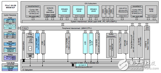
图1.PSoC 62系列框图

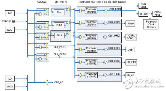
图2.PSoC 62系列时钟框图
PSoC 6 Wi-Fi BT原型套件CY8CPROTO-062-4343W
The PSoC 6 Wi-Fi BT Prototyping Kit (CY8CPROTO-062-4343W) is a low-cost hardware platform that enables design and debug of PSoC 6 MCUs. It comes with a CY8CMOD-062-4343W daughter card, industry-leading CapSense® for touch buttons and slider, on-board debugger/programmer with KitProg3, MicroSD card interface, 512-Mb Quad-SPI NOR flash, PDM microphone, and a thermistor. It also includes a Murata LBEE5KL1DX module, based on the CYW4343W combo device.
Featuring the PSoC 62 MCU, providing up to 2MB flash and 1MB SRAM
PSoC 6 is purpose-built for the IoT, delivering the industry’s lowest power, most flexibility, and built-in security for the IoT. It delivers dual-cores, with a 150-MHz Arm® Cortex®-M4 as the primary application processor and a 100-MHz Arm Cortex-M0+ as the secondary processor for low-power operations. To find out about the unique and differentiating features of our PSoC 6 MCUs, please visit the PSoC 6 product page.
-
汽车级PSoC™ 4:PSoC™ 4000S系列深度剖析2025-12-19 472
-
如何在PSoC62 Evaluation kit开发板上运行RT-Thread呢?2024-02-27 3019
-
PSoC62如何获取系统时钟?2024-02-21 947
-
基于PSoC62开发板的智能室内环境监测系统2023-07-31 3012
-
基于PSOC62 CAPSENSE evaluation kit板的环境盒子设计实现2023-07-22 2027
-
基于PSOC62 CAPSENSE evaluation kit的远程空调遥控器设计2023-07-19 1589
-
英飞凌PSoC62 实现超低功耗温湿度计2023-06-03 2666
-
大数据平台架构与建设思路2021-03-24 1559
-
SiFive Shield: 一个开放的、可扩展的安全平台架构2020-08-13 4519
-
Cypress PSoC 4200DS可配置电源平台解决方案2019-04-18 1685
-
基于Eclipse平台架构技术分析及基于RCP的应用2017-10-30 1321
-
中文版器件数据手册PSoC 4 可编程片上系统 (PSoC®)2013-07-04 10977
全部0条评论

快来发表一下你的评论吧 !

