

ADI ADP2450 断路器电源管理IC解决方案
嵌入式技术
描述
ADI公司的ADP2450是专用的电流变压器(CT)取电控制器,集成了带电源检测的升压分流控制器,高效降压稳压器,四个低失调低功耗可编增益放大器(PGA),一个低失调运放,一个快速模拟解扣电路和一个执行器驱动器,输入电压4.5V-46V,可调输出电压4.5V-36V,可低至0.6V,连续输出电流500mA,固定开关频率1.2MHz,主要用在低压电路断路器和电流变压器(CT)电源.本文介绍了ADP2450主要特性,功能框图,应用电流以及评估板ADP2450ACPZ-3-EVBZ主要特性,电路图,材料清单和PCB设计图.
The ADP2450 integrates one boost shunt controller with powerdetection, one high efficiency buck regulator, four low offset,low power consumption programmable gain amplifiers (PGAs),one low offset operation amplifier, a fast analog trip circuit, and an actuator driver. The ADP2450 is targeted for low voltagecircuit breaker, such as molded case circuit breaker (MCCB),and CT powered supply applications. The boost output voltage can be up to 36 V and integrates apower detection circuit that prevents the circuit from powerhiccups. The power detection threshold is programmable with resistors.
The buck regulator operates over a wide input voltage rangefrom 4.5 V to 36 V, and the output voltage can be adjusted downto 0.6 V. The buck regulator provides output currents of up to 500 mA. The buck regulator works in pulse-width modulation (PWM) mode with a fixed 1.2 MHz switching frequency, providing low output ripple voltage to the system. The output voltage of buck regulator is monitored by thesupervisory circuit. When the output voltage is below themonitoring threshold, the reset signal is pulled low and can be used to reset the microprocessor. The supervisory circuit makes the system more reliable. The ADP2450 integrates four low offset, low power consumptionamplifiers. With the programmable gain features, the ADP2450 provides accuracy measurement over a wide current input range. A low offset operation amplifier is integrated in the ADP2450for leakage current detection. The ADP2450 also integrates an analog trip circuit, whichprovides fast trip response and enhances system reliability. Additional protection includes buck overcurrent protection (OCP) and system thermal shutdown (TSD).
The ADP2450 operates over the −40℃ to +125℃ junction temperature range and is available in a 32-lead LFCSP package.
ADP2450主要特性:
Boost shunt controller
Adjustable output voltage range: 4.5 V to 36 V
Integrated boost shunt driver
Programmable power detection threshold
Buck regulator
Input voltage range: 4.5 V to 36 V
Continuous output current: 500 mA
Adjustable output voltage down to 0.6 V
Fixed output options: 3.3 V and 5 V
1.2 MHz fixed switching frequency
Voltage monitoring and open-drain reset output
4 programmable gain amplifiers
Low power consumption
Programmable gain and output dc common voltage
Low offset operation amplifier for leakage and groundingfault current detection
Analog trip circuit with programmable trip threshold
Actuator driver output
ADP2450应用:
Low voltage circuit breaker
Current transformer (CT) powered supply
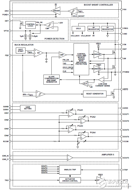
图1.ADP2450功能框图
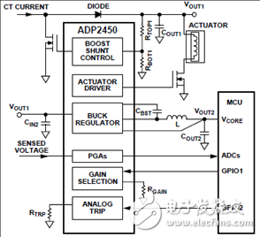
图2.ADP2450典型应用电路图
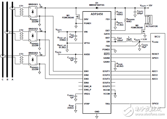
图3.ADP2450单圈三相检测设计案例电路图
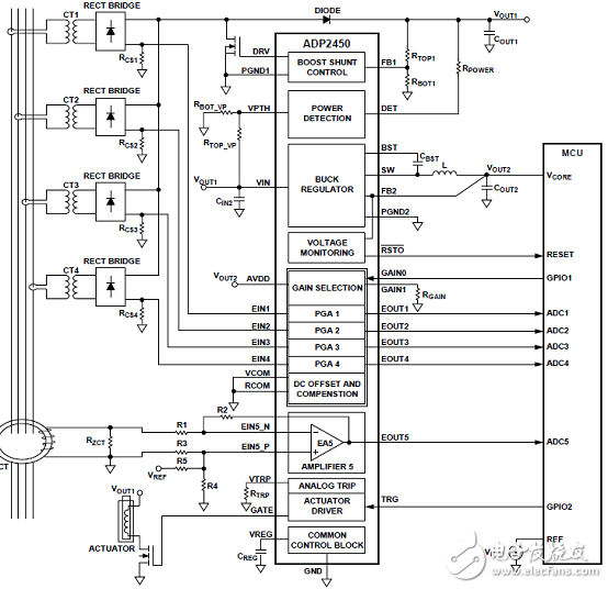
图4.ADP2450单圈,信号和电源共享同一CT的应用电路图
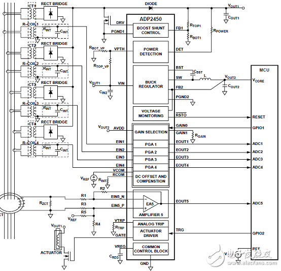
图5.ADP2450双圈,CT提供电源和Rogowski(洛氏线圈)提供信号的应用电路图
评估板ADP2450ACPZ-3-EVBZ
The ADP2450ACPZ-3-EVBZ evaluation board provides a complete and compact solution that allows users to evaluate the performance of the ADP2450 with a near ideal printed circuit board (PCB) layout. The evaluation board is compatible with current transformer (CT) or ac current source as its input power source. The main device on the evaluation board, the ADP2450, integrates a boost shunt controller with power detection, a high efficiency buck regulator, four low offset and low power consumption programmable gain amplifiers (PGAs), a low offset operation amplifier, a fast analog trip circuit, and an actuator driver. With an external microcontroller unit (MCU) connected, the evaluation board is suitable for quick system evaluation of circuit breaker applications. Full details on the ADP2450 are provided in the ADP2450 data sheet, available from Analog Devices, Inc. Consult the data sheet in conjunction with this user guide when working with the ADP2450ACPZ-3-EVBZ.
评估板ADP2450ACPZ-3-EVBZ主要特性:
Full featured evaluation board for the ADP2450
Compact solution size
4-layer high glass transition temperature (TG) PCB for superior thermal performance
Connections through vertical printed circuit tail pin headers
Compatible with ac current source input or CT input
Supports single coil and dual coil application
Adjustable output for buck regulator
On-board precision reference
On-board PGA gain setting
Supports analog trip function
Supports power detection function
Voltage monitor and reset output
Flexible connection with external MCU
评估板ADP2450ACPZ-3-EVBZ应用:
Full evaluation of ADP2450
EVALUATION KIT CONTENTS
ADP2450ACPZ-3-EVBZ evaluation board
图6.评估板ADP2450ACPZ-3-EVBZ外形图
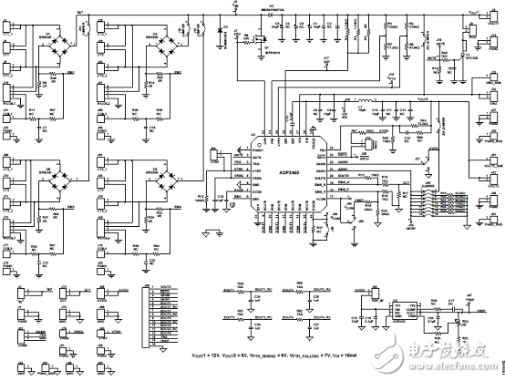
图7.评估板ADP2450ACPZ-3-EVBZ电路图
评估板ADP2450ACPZ-3-EVBZ材料清单:

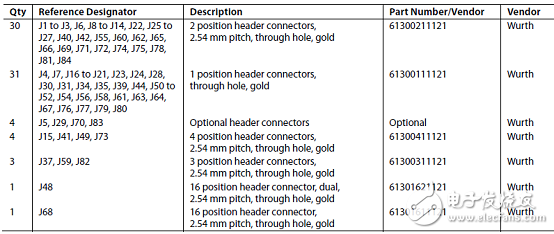
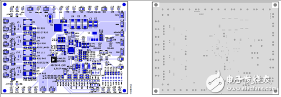
图8.评估板ADP2450ACPZ-3-EVBZ PCB设计图:左:元件面;右:层2,地面,
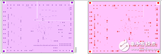
图9.评估板ADP2450ACPZ-3-EVBZ PCB设计图:左:层3,电源面;右:层4,底面,
-
ADP2450:电路断路器应用的高效电源管理IC2026-02-05 263
-
EVAL-ADP2450 EVAL-ADP2450评估板2021-07-14 286
-
ADP2450:适用于断路器的电源管理IC产品手册2021-05-08 826
-
智能断路器应用方案之智慧路灯杆应用方案2020-10-31 2217
-
智能断路器应用方案之银行智慧用电2020-09-19 2519
-
智能断路器应用方案之学校智慧用电2020-09-11 2618
-
PCS控制电源断路器跳闸的解决方案2020-09-01 3346
-
智能电表外置微型断路器解决方案2019-07-24 3282
-
如何测试断路器2019-03-22 3326
-
ADP2450 用于断路器应用的电源管理 IC2019-02-22 615
-
Ameya360 智能漏电断路器模块解决方案2018-12-10 1650
-
ADI可穿戴设备电源管理解决方案2018-09-17 3129
-
断路器基本知识2013-05-23 4161
-
ADI推出ADP5034高集成度电源管理芯片调节器/LDO2011-07-29 3900
全部0条评论

快来发表一下你的评论吧 !

