

STM32L496xx系列超低功耗32位ARM MCU开发方案
ARM
描述
ST公司的STM32L496xx系列是超低功耗32位ARM MCU+FPU,工作频率高达80MHz,具有100DMIPS,集成了多达1MB闪存,320KB SRAM,USB OTG FS,提供多达三个快速12位ADC(5 Msps),两个比较器,两个运放,两个DAC通路,一个内部基准电压缓冲器,一个低功耗RTC,两个通用32位计时器和两个专用马达控制的16位低功耗计时器,七个通用16位计时器和两个16位低功耗计时器。主要用在包括音频和图像等低功耗的应用。本文介绍了STM32L496xx系列主要特性,框图以及时钟树框图和评估板32L496GDISCOVERY Discovery kit框图,主要特性和电路图以及PCB元件布局图。
The STM32L496xx devices are the ultra-low-power microcontrollers based on the high-performance ARM® Cortex®-M4 32-bit RISC core operating at a frequency of up to 80 MHz. The Cortex-M4 core features a Floating point unit (FPU) single precision which supports all ARM single-precision data-processing instructions and data types. It also implements a full set of DSP instructions and a memory protection unit (MPU) which enhances application security.
The STM32L496xx devices are the ultra-low-power microcontrollers based on the high-performance Arm® Cortex®-M4 32-bit RISC core operating at a frequency of up to 80 MHz. The Cortex-M4 core features a Floating point unit (FPU) single precision which supports all Arm® single-precision data-processing instructions and data types. It also implements a full set of DSP instructions and a memory protection unit (MPU) which enhances application security.
The STM32L496xx devices embed high-speed memories (up to 1 Mbyte of Flash memory, 320 Kbyte of SRAM), a flexible external memory controller (FSMC) for static memories (for devices with packages of 100 pins and more), a Quad SPI flash memories interface (available on all packages) and an extensive range of enhanced I/Os and peripherals connected to two APB buses, two AHB buses and a 32-bit multi-AHB bus matrix.
The STM32L496xx devices embed several protection mechanisms for embedded Flash memory and SRAM: readout protection, write protection, proprietary code readout protection and Firewall.
The devices offer up to three fast 12-bit ADCs (5 Msps), two comparators, two operational amplifiers, two DAC channels, an internal voltage reference buffer, a low-power RTC, two general-purpose 32-bit timer, two 16-bit PWM timers dedicated to motor control, seven general-purpose 16-bit timers, and two 16-bit low-power timers. The devices support four digital filters for external sigma delta modulators (DFSDM)。
In addition, up to 24 capacitive sensing channels are available. The devices also embed an integrated LCD driver 8x40 or 4x44, with internal step-up converter.They also feature standard and advanced communication interfaces.
• Four I2Cs
• Three SPIs
• Three USARTs, two UARTs and one Low-Power UART.
• Two SAIs (Serial Audio Interfaces)
• One SDMMC
• Two CAN
• One USB OTG full-speed
• One SWPMI (Single Wire protocol Master Interface)
• Camera interface
• DMA2D controller
The STM32L496xx operates in the -40 to +85℃ (+105℃ junction), -40 to +125℃ (+130℃ junction) temperature ranges from a 1.71 to 3.6 V VDD power supply when using internal LDO regulator and a 1.05 to 1.32V VDD12 power supply when using external SMPS supply. A comprehensive set of power-saving modes allows the design of low-power applications.
Some independent power supplies are supported: analog independent supply input for ADC, DAC, OPAMPs and comparators, 3.3 V dedicated supply input for USB and up to 14 I/Os can be supplied independently down to 1.08V. A VBAT input allows to backup the RTC and backup registers. Dedicated VDD12 power supplies can be used to bypass the internal LDO regulator when connected to an external The STM32L496xx family offers six packages from 64-pin to 169-pin packages.
STM32L496xx系列主要特性:
• Ultra-low-power with FlexPowerControl
– 1.71 V to 3.6 V power supply
– -40 ℃ to 85/125 ℃ temperature range
– 320 nA in VBAT mode: supply for RTC and 32x32-bit backup registers
– 25 nA Shutdown mode (5 wakeup pins)
– 108 nA Standby mode (5 wakeup pins)
– 426 nA Standby mode with RTC
– 2.57 μA Stop 2 mode, 2.86 μA Stop 2 with RTC
– 91 μA/MHz run mode (LDO Mode)
– 37 μA/MHz run mode (@3.3 V SMPS Mode)
– Batch acquisition mode (BAM)
– 5 μs wakeup from Stop mode
– Brown out reset (BOR) in all modes except shutdown
– Interconnect matrix
• Core: Arm® 32-bit Cortex®-M4 CPU with FPU, Adaptive real-time accelerator (ART Accelerator™) allowing 0-wait-state execution from Flash memory, frequency up to 80 MHz, MPU, 100 DMIPS and DSP instructions
• Performance benchmark
– 1.25 DMIPS/MHz (Drystone 2.1)
– 273.55 Coremark® (3.42 Coremark/MHz @ 80 MHz)
• Energy benchmark
– 279 ULPMark™ CP score
– 80.2 ULPMark™ PP score
• 16 x timers: 2 x 16-bit advanced motor-control, 2 x 32-bit and 5 x 16-bit general purpose, 2 x 16-bit basic, 2 x low-power 16-bit timers (available in Stop mode), 2 x watchdogs, SysTick timer
• RTC with HW calendar, alarms and calibration
• Up to 136 fast I/Os, most 5 V-tolerant, up to 14 I/Os with independent supply down to 1.08 V
• Dedicated Chrom-ART Accelerator™ for enhanced graphic content creation (DMA2D)
• 8- to 14-bit camera interface up to 32 MHz (black&white) or 10 MHz (color)
• Memories
– Up to 1 MB Flash, 2 banks read-while-write, proprietary code readout protection
– 320 KB of SRAM including 64 KB with hardware parity check
– External memory interface for static memories supporting SRAM, PSRAM, NOR and NAND memories
– Dual-flash Quad SPI memory interface
• Clock Sources
– 4 to 48 MHz crystal oscillator
– 32 kHz crystal oscillator for RTC (LSE)
– Internal 16 MHz factory-trimmed RC (±1%)
– Internal low-power 32 kHz RC (±5%)
– Internal multispeed 100 kHz to 48 MHz oscillator, auto-trimmed by LSE (better than ±0.25% accuracy)
– Internal 48 MHz with clock recovery
– 3 PLLs for system clock, USB, audio, ADC
• LCD 8 × 40 or 4 × 44 with step-up converter
• Up to 24 capacitive sensing channels: support touchkey, linear and rotary touch sensors
• 4 x digital filters for sigma delta modulator
• Rich analog peripherals (independent supply)
– 3 × 12-bit ADC 5 Msps, up to 16-bit with hardware oversampling, 200 μA/Msps
– 2 x 12-bit DAC output channels, low-power sample and hold
– 2 x operational amplifiers with built-in PGA
– 2 x ultra-low-power comparators
• 20 x communication interfaces
– USB OTG 2.0 full-speed, LPM and BCD
– 2 x SAIs (serial audio interface)
– 4 x I2C FM+(1 Mbit/s), SMBus/PMBus
– 5 x U(S)ARTs (ISO 7816, LIN, IrDA, modem)
– 1 x LPUART
– 3 x SPIs (4 x SPIs with the Quad SPI)
– 2 x CAN (2.0B Active) and SDMMC
– SWPMI single wire protocol master I/F
– IRTIM (Infrared interface)
• 14-channel DMA controller
• True random number generator
• CRC calculation unit, 96-bit unique ID
• Development support: serial wire debug (SWD), JTAG, Embedded Trace Macrocell™
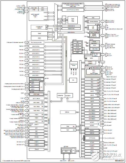
图1.STM32L496xx系列框图
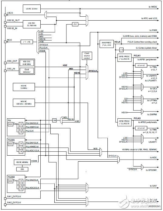
图2.STM32L496xx系列时钟树框图
评估板32L496GDISCOVERY Discovery kit
The 32L496GDISCOVERY Discovery kit is a complete demonstration and development platform for the STMicroelectronics ARM® Cortex®-M4 core-based STM32L496AGI6 microcontroller. Thanks to the innovative ultra-low-power oriented features, extended RAM and graphics performance (Chrom-ART Accelerator™) offered by the STM32L496AG, the 32L496GDISCOVERY kit is designed to enable easy prototyping for many applications, including audio and graphics, with state-of-the-art energy efficiency. For even more user-friendliness, the on-board ST-LINK/V2-1 debugger provides out-of-the-box loading and debugging capabilities. The microcontroller features the following interfaces: four I2Cs, three SPIs, one SDIO, FMC and Quad-SPI. It also features five USARTs, one ULP UART, two CAN buses, three 12-bit ADCs, two 12-bit DACs, two SAIs, two ULP analog comparators, two Op Amps, LCD 8 × 40 or 4 × 44 with step-up converter, four digital filters for sigma delta modulator and SWP, 8- to 14-bit camera interface, USB 2.0 OTG FS, JTAG and SWD debugging support. This 32L496GDISCOVERY Discovery kit offers everything required for users to get started quickly and develop applications easily.
The full range of hardware features on the board helps users to evaluate almost all peripherals (USB OTG FS, microSD™ card, 8-bit camera, 8-Mbit PSRAM, IDD measurement, full-duplex I2S with an audio CODEC and stereo jack for headset including analog microphone, DFSDM with a pair of MEMS digital microphones on board, Quad-SPI Flash memory device, 1.54-inch TFT LCD using FMC interface with capacitive touch panel and others) and develop applications. Arduino™ Uno V3, PMOD and STMod+ connectors allow easy connection of extension shields or daughterboards for specific applications.
The integrated ST-LINK/V2-1 provides an embedded in-circuit debugger and programmer for the STM32 MCU.
The 32L496GDISCOVERY Discovery kit comes with the STM32 comprehensive software HAL library and LL APIs together with various packaged software examples.
图2.评估板32L496GDISCOVERY Discovery kit外形图(顶视图)
图3.评估板32L496GDISCOVERY Discovery kit外形图(底视图)
评估板32L496GDISCOVERY Discovery kit主要特性:
• STM32L496AGI6 Arm®(a) Cortex®-M4 core-based microcontroller featuring 1 Mbyte of Flash memory and 320 Kbytes of RAM in an UFBGA169 package
• 1.54-inch 240 x 240 pixel-TFT color LCD with parallel interface
• SAI Audio CODEC, with a stereo headset jack, including analog microphone input
• Stereo digital MEMS microphones
• 8-Mbit PSRAM
• IDD measurement
• 64-Mbit Quad-SPI Flash
• 8 LEDs, including 3 user controllable ones
• Reset push button
• 4-direction joystick with selection
• microSD™ card connector (card included)
• Camera 8-bit connector
• STMod+ and PMOD connectors
• USB OTG FS with Micro-AB connector
• Compatible Arduino™ Uno V3 connectors
• 5 source options for power supply
– ST-LINK/V2-1 USB connector
– User USB FS connector
– VIN from Arduino™ connector
– 5 V from Arduino™ connector
– USB charger
• 2 possible supply voltages for the MCU: 1.8 V and 3.3 V
• On-board ST-LINK/V2-1 debugger/programmer with USB re-enumeration capability: mass storage, virtual COM port
• Comprehensive free software including a variety of examples, part of the STM32Cube package
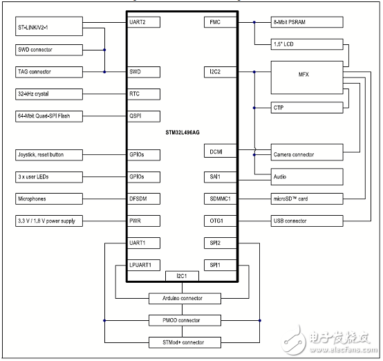
图4.评估板32L496GDISCOVERY Discovery kit硬件框图
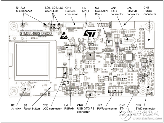
图5.评估板32L496GDISCOVERY Discovery kit元件分布图(顶层)
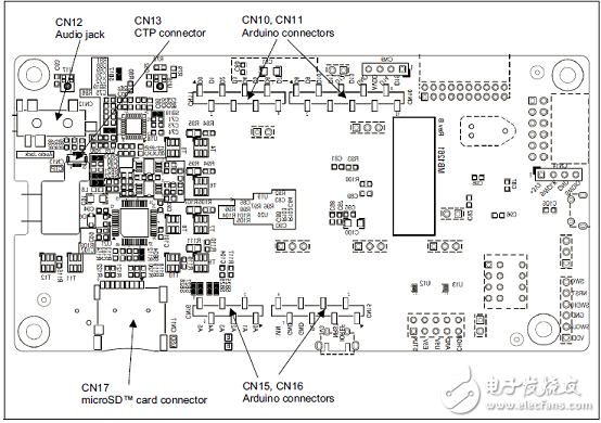
图6.评估板32L496GDISCOVERY Discovery kit元件分布图(底层)
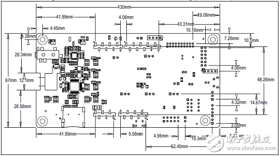
图7.评估板32L496GDISCOVERY Discovery kit机械尺寸图(底层)
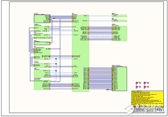
图8.评估板32L496GDISCOVERY Discovery kit电路图(1)
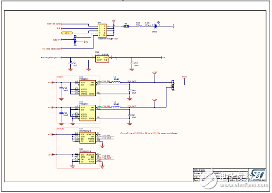
图9.评估板32L496GDISCOVERY Discovery kit电路图(2)
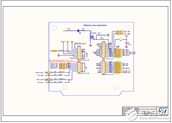
图10.评估板32L496GDISCOVERY Discovery kit电路图(3)
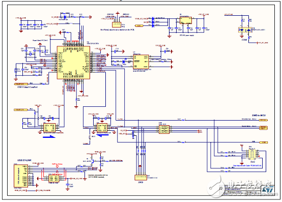
图11.评估板32L496GDISCOVERY Discovery kit电路图(4)
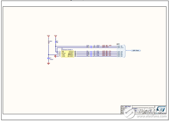
图12.评估板32L496GDISCOVERY Discovery kit电路图(5)
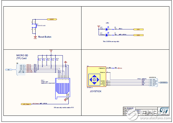
图13.评估板32L496GDISCOVERY Discovery kit电路图(6)
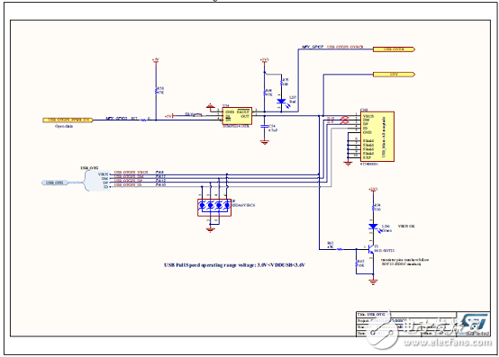
图14.评估板32L496GDISCOVERY Discovery kit电路图(7
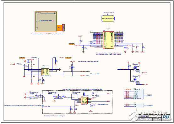
图15.评估板32L496GDISCOVERY Discovery kit电路图(8)
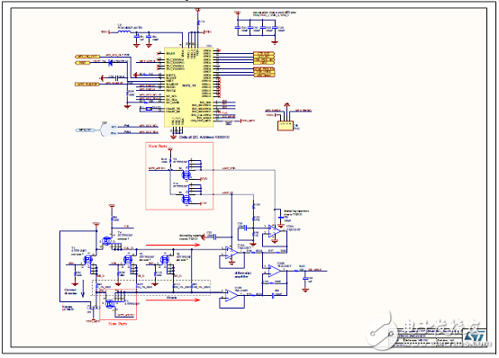
图16.评估板32L496GDISCOVERY Discovery kit电路图(9)
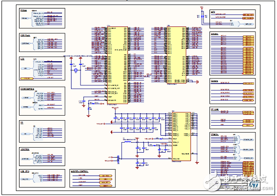
图17.评估板32L496GDISCOVERY Discovery kit电路图(10)
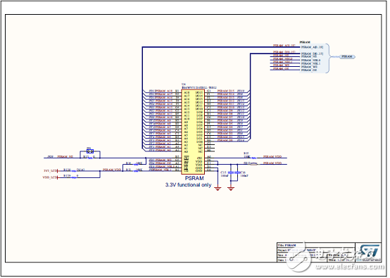
图18.评估板32L496GDISCOVERY Discovery kit电路图(11)
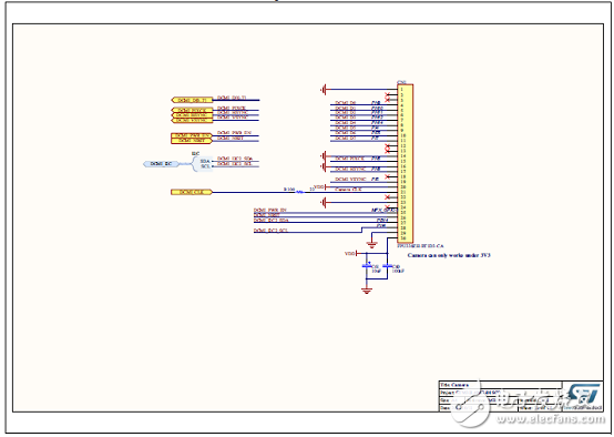
图19.评估板32L496GDISCOVERY Discovery kit电路图(12)
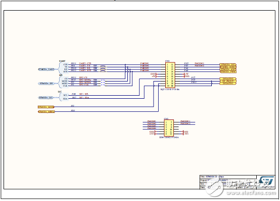
图20.评估板32L496GDISCOVERY Discovery kit电路图(13)
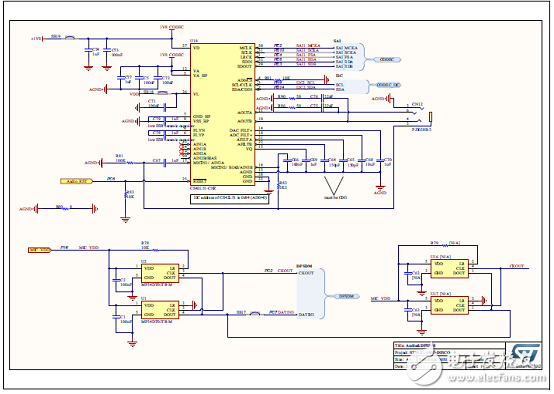
图21.评估板32L496GDISCOVERY Discovery kit电路图(14)
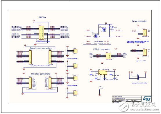
图22.评估板32L496GDISCOVERY Discovery kit电路图(15)
详情请见:
https://www.st.com/content/ccc/resource/technical/document/datasheet/group3/3f/73/19
/d1/d4/9e/48/34/DM00284211/files/DM00284211.pdf/jcr:content/translations/en.DM00284211.pdf
和https://www.st.com/content/ccc/resource/technical/document/user_manual/group0/1f/0f/b1/86
/ef/c7/45/84/DM00353127/files/DM00353127.pdf/jcr:content/translations/en.DM00353127.pdf
en.DM00284211.pdf
-
探索STM32L072xx:超低功耗32位MCU的卓越之选2026-04-18 230
-
STM32L073xx:超低功耗32位MCU的卓越之选2026-03-17 529
-
STM32L071xx:超低功耗32位MCU的技术剖析与应用指南2026-03-15 1249
-
STM32L072xx:超低功耗32位MCU的卓越之选2026-03-03 1394
-
STM32L072xx:超低功耗32位MCU的设计指南与应用潜力2026-03-02 936
-
STM32L496xx/STM32L4A6xx设备勘误表2022-11-30 463
-
DS11585 STM32L494XX微控制器数据手册2022-11-24 548
-
RM0451_超低功耗 STM32L0x0 先进的基于 Arm® 的 32 位 MCU2022-11-23 740
-
AN4822_STM32L476xx、486xx和STM32L496xx、4A6xx微控制器之间的移植2022-11-21 1010
-
STM32L151XX和STM32L152XX超低功耗32位MCU Cortex的数据手册免费下载2020-01-14 1744
全部0条评论

快来发表一下你的评论吧 !
