

TI LMG3410R050 GaN功率放大级解决方案
嵌入式技术
描述
TI公司的LMG3410R050是具有过流保护的600-V 50-mΩ GaN功率放大级,比硅MOSFET具有固有的优势包括超低输入和输出电容,零反向恢复以降低开关损耗达80%之多,以及低开关节点振铃以降低EMI,20ns传输时延用于MHz工作,25-100V/ns用户可调转换速率,具有强健的保护,不需要外接保护元件,主要用在高密度工业和消费类电源,多级转换器,太阳能逆变器,工业马达驱动,不间断电源(UPS)以及高压电池充电器.本文介绍了LMG3410R050主要特性, 功能框图和应用电路,以及评估板LMG3410EVM-018和LMG34xx-BB-EVM主要特性和指标,电路图,材料清单和PCB设计图.
The LMG3410R050 GaN power stage with integrated driver and protection enables designers to achieve new levels of power density and efficiency in power electronics systems. The LMG3410’s inherent advantages over silicon MOSFETs include ultra-low
input and output capacitance, zero reverse recovery to reduce switching losses by as much as 80%, and low switch node ringing to reduce EMI. These advantages enable dense and efficient topologies like the totem-pole PFC.
The LMG3410R050 provides a smart alternative to traditional cascode GaN and standalone GaN FETs by integrating a unique set of features to simplify design, maximize reliability and optimize the performance of any power supply. Integrated gate drive enables 100V/ns switching with near zero Vds ringing, <100 ns current limiting self-protects against unintended shoot-through events, Overtemperature shutdown prevents thermal runaway, and system interface signals provide self-monitoring capability.
LMG3410R050 is a high-performance 600-V GaN transistor with integrated gate driver. The GaN transistor provides ultra-low input and output capacitance and zero reverse recovery. The lack of reverse recovery enables efficient operation in half-bridge and bridge-based topologies.
TI utilizes a Direct Drive architecture to control the GaN FET within the LMG3410R050. When the driver is powered up, the GaN FET is controlled directly with the integrated gate driver. This architecture provides superior switching performance compared with the traditional cascode approach.
The integrated driver solves a number of challenges using GaN devices. The LMG3410R050 contains a driver specifically tuned to the GaN device for fast driving without ringing on the gate. The driver ensures the device stays off for high drain slew rates up to 150 V/ns. In addition, the integrated driver protects against faults by providing overcurrent and overtemperature protection. This feature can protect the system in case of a device failure, or prevent a device failure in the case of a controller error or malfunction.
Unlike silicon MOSFETs, there is no p-n junction from source to drain in GaN devices. That is why GaN devices have no reverse recovery losses. However, the GaN device can still conduct from source to drain in 3rd quadrant of operation similar to a body diode but with higher voltage drop and higher conduction loss. 3rd quadrant operation can be defined as follows; when the GaN device is turned off and negative current pulls the drain node voltage to be lower than its source. The voltage drop across GaN device during 3rd quadrant operation is high; therefore, it is recommended to operate with synchronous switching and keep the duration of 3rd quadrant operation at minimum.
LMG3410R050主要特性:
1• TI GaN Process Qualified Through Accelerated Reliability In-application Hard-switching Mission Profiles
• Enables High Density Power Conversion Designs
– Superior System Performance Over Cascode or Stand-alone GaN FETs
– Low Inductance 8mm x 8mm QFN Package for Ease of Design, and Layout
– Adjustable Drive Strength for Switching
Performance and EMI Control
– Digital Fault Status Output Signal
– Only +12 V Unregulated Supply Needed
• Integrated Gate Driver
– Zero Common Source Inductance
– 20 ns Propagation Delay for MHz Operation
– Process-tuned Gate Bias Voltage for Reliability
– 25 to 100V/ns User Adjustable Slew Rate
• Robust Protection
– Requires No External Protection Components
– Overcurrent Protection with <100ns Response
– >150V/ns Slew Rate Immunity
– Transient Overvoltage Immunity
– Overtemperature Protection
– UVLO Protection on All Supply Rails
LMG3410R050应用:
• High Density Industrial and Consumer Power Supplies
• Multi-level Converters
• Solar Inverters
• Industrial Motor Drives
• Uninterruptable Power Supplies
• High Voltage Battery Chargers
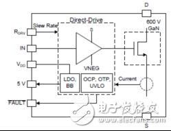
图1. LMG3410R050简化框图
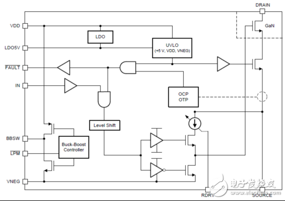
图2. LMG3410R050功能框图
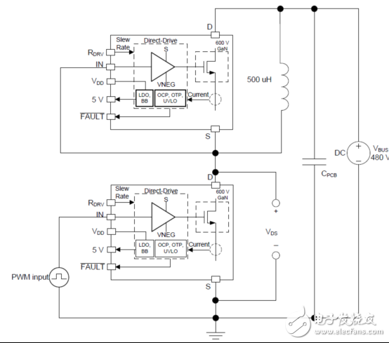
图3. LMG3410R050用来确定开关参数的电路图
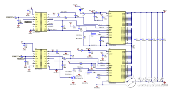
图4. LMG3410R050应用电路图
评估板LMG3410EVM-018
The LMG3410EVM-018 features two LMG3410R050 600V GaN power transistors with integrated drivers that are configured in a half bridge with all the required bias circuit and logic/power level shifting. Essential power stage and gate driving high frequency current loops are fully enclosed on the board to minimize parasitic inductances, reducing voltage overshoots and improving performance. The LMG3410EVM-018 is configured to have a socket style external connection for easy interface with external power stages to run the LMG3410R050 in various applications.
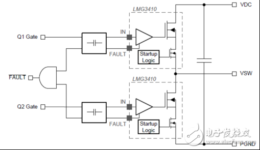
图5.评估板LMG3410EVM-018简化电路
图6.评估板LMG3410EVM-018外形图(顶视)
图7.评估板LMG3410EVM-018外形图(底视)
评估板LMG3410EVM-018主要特性和指标:
• Two options to bias the LMG3410, isolated power or from bootstrap diode
• Over temperature, overcurrent, and under voltage lockout protection with FAULT indication that is level shifted to an AGND referenced signal
• Gate logic input support of either 3.3V or 5V logic
• Maximum recommended operating voltage of 480V and absolute maximum voltage of 600V
评估板LMG34xx-BB-EVM主要特性和指标:
• Requires only a single 12V bias supply
• Requires only a single 0V to 5V PWM input to generate gate drive signal
• PWM disable in the event of a fault from the LMG3410EVM-018
• Maximum recommended operating voltage of 480V and absolute maximum voltage of 600V
• Maximum recommended operating inductor current of 8A
The LMG3410EVM-018 is designed for use in AC/DC, DC/DC and DC/AC applications
• Totem-Pole PFC converters
• Phase-Shifted Full Bridge or LLC Converter
• Buck converter such as the LMG34XX-BB-EVM
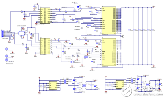
图8.评估板LMG3410EVM-018电路图
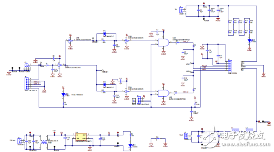
图9.评估板LMG34xx-BB-EVM电路图
评估板LMG3410EVM-018材料清单:

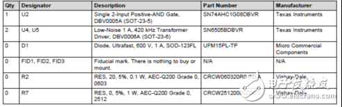
评估板LMG34XX-BB-EVM-018材料清单
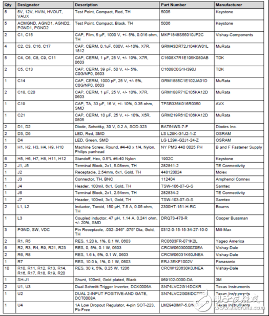
图10. 评估板LMG3410EVM-018和LMG34XX-BB-EVM连接图
图11. 评估板LMG3410EVM-018 PCB设计图:左:内部铜层2;右:底层和元件
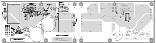
图12. 评估板LMG34XX-BB-EVM PCB设计图:左:顶层和元件;右:底层和元件
-
深度解析LMG342xR050:600V 50mΩ GaN FET的卓越性能与应用2026-03-01 810
-
LMG3410R070RWHR 高性能 GaN 功率器件2025-11-29 450
-
技术资料#LMG3410R050 具有集成驱动器和保护功能的 600V 50mΩ GaN2025-02-26 1263
-
LMG3410R150-031 EVM用户指南2025-02-25 1194
-
正确驱动LMG5200 GaN功率级的步骤2022-11-17 832
-
基于GaN的CrM模式的图腾柱无桥PFC参考方案的设计2022-01-20 3070
-
支持高密度电源转换设计的TI LMG341xR050 GaN2020-05-29 3788
-
TI LMG341xR050 GaN功率级在贸泽开售 支持高密度电源转换设计2020-04-13 1930
-
在GaN解决方案门户上查看TI完整的GaN直流/直流转换产品组合2019-07-29 2912
-
LMG3410R070 具有集成驱动器和保护功能的 600V 70mΩ GaN2019-01-08 663
-
LMG3410 LMG3410 Spitfire - 具有集成驱动器和安全开关的智能 GaN FET2018-11-02 1332
-
基于GaN的高效率CrM图腾柱PFC转换器包括BOM及层图2018-10-25 3779
全部0条评论

快来发表一下你的评论吧 !
