
Cypress PSoC 4200DS可配置电源平台解决方案
嵌入式技术
描述
cypress公司的PSoC 4200DS是可升级和可配置的具有ARM® Cortex™-M0 CPU的可编程嵌入系统控制器平台架构,包括有可编程和可配置模拟和数字区块以及灵活的自动走线,组合了MCU和可编程数字可编程逻辑,可编程互连,标准通信和定时外设,支持编程,测试,调试和硬件和固件的跟踪.本文介绍了PSoC 4200DS主要特性,框图,以及原型板CY8CKIT-146PSoC 4200DS主要特性,电路图,材料清单,PCB设计图和装配图.
PSoC® 4 is a scalable and reconfigurable platform architecture for a family of programmable embedded system controllers with anARM® Cortex™-M0 CPU. It combines programmable and reconfigurable analog and digital blocks with flexible automatic routing. ThePSoC 4200DS product family, based on this platform architecture, is a combination of a microcontroller with digital programmablelogic, programmable interconnect, and standard communication and timing peripherals. The PSoC 4200DS products will be fullycompatible with members of the PSoC 4 platform for new applications and design needs. The programmable digital subsystem allowsflexibility and in-field tuning of the design.
The PSoC 4200DS devices include extensive support forprogramming, testing, debugging, and tracing both hardwareand firmware.The ARM Serial_Wire Debug (SWD) interface supports allprogramming and debug features of the device.
Complete debug-on-chip functionality enables full-devicedebugging in the final system using the standard productiondevice. It does not require special interfaces, debugging pods,simulators, or emulators. Only the standard programmingconnections are required to fully support debug.
The PSoC Creator Integrated Development Environment (IDE)provides fully integrated programming and debug support forPSoC 4200DS devices. The SWD interface is fully compatiblewith industry-standard third-party tools. The PSoC 4200DSfamily provides a level of security not possible with multi-chipapplication solutions or with microcontrollers. This is due to itsability to disable debug features, robust flash protection, andbecause it allows customer-proprietary functionality to be implementedin on-chip programmable blocks.
The debug circuits are enabled by default and can only bedisabled in firmware. If not enabled, the only way to re-enablethem is to erase the entire device, clear flash protection, andreprogram the device with new firmware that enables debugging.
Additionally, all device interfaces can be permanently disabled(device security) for applications concerned about phishingattacks due to a maliciously reprogrammed device or attempts todefeat security by starting and interrupting flash programmingsequences. Because all programming, debug, and test interfacesare disabled when maximum device security is enabled,PSoC 4200DS with device security enabled may not be returnedfor failure analysis. This is a trade-off the PSoC 4200DS allowsthe customer to make.
PSoC 4200DS主要特性:
32-bit MCU Subsystem
■ 48 MHz ARM Cortex-M0 CPU with single-cycle multiply
■ Up to 64 kB of flash with Read Accelerator
■ Up to 8 kB of SRAM
■ DMA engine
Programmable Digital
■ Four programmable logic blocks, each with 8 Macrocells andan 8-bit data path (called universal digital blocks or UDBs)
■ Programmable I/O block (PRGIO) provides the ability toperform Boolean functions in the I/O signal path
■ Cypress-provided peripheral component library, user-definedstate machines, and Verilog input
Low Power 1.71 to 5.5 V Operation
■ Low-power Deep Sleep Mode with GPIO pin wakeup
Serial Communication
■ Three independent run-time reconfigurable serialcommunication blocks (SCBs) with reconfigurable I2C, SPI, orUART functionality
Timing and Pulse-Width Modulation
■ Four 16-bit timer/counter pulse-width modulator (TCPWM)blocks
■ Center-aligned, Edge, and Pseudo-random modes
■ Comparator-based triggering of Kill signals for motor drive andother high-reliability digital logic applications
Packages
■ 25-ball CSP package 2.07 mm × 2.11 mm, 28-pin SSOPpackage.
■ Up to 21 programmable GPIOs
■ GPIO drive modes, strengths, and slew rates are programmable
PSoC Creator Design Environment
■ Integrated Development Environment (IDE) providesschematic design entry and build (with analog and digitalautomatic routing)
■ Applications Programming Interface (API component) for allfixed-function and programmable peripherals
Industry-Standard Tool Compatibility
■ After schematic entry, development can be done withARM-based industry-standard development tools

图1.PSoC 4200DS框图
原型板CY8CKIT-146PSoC 4200DS
The CY8CKIT-146 PSoC 4200DS prototyping Kit is intended for use as a development platform forhardware or software in a laboratory environment. The board is an open system design, which doesnot include a shielded enclosure. This may cause interference to other electrical or electronicdevices in close proximity. In a domestic environment, this product may cause radio interference. Insuch cases, you may be required to take adequate preventive measures. In addition, this boardshould not be used near any medical equipment or RF devices.
Attaching additional wiring to this product or modifying the product operation from the factory defaultsettings may affect its performance and cause interference with other apparatus in the immediatevicinity. If such interference is detected, suitable mitigating measures should be taken.
The PSoC 4200DS Prototyping Kit, as shippedfrom the factory, has been verified to meet withrequirements of CE as a Class A product.
Thank you for your interest in the CY8CKIT-146 PSoC 4200DS Prototyping Kit. The PSoC 4200DSprototyping kit is designed as an easy-to-use and inexpensive prototyping platform. ThePSoC 4200DS Prototyping Kit supports the PSoC 4200DS device family, delivering a completesystem solution for a wide range of embedded applications at a very low cost. The PSoC 4200DSdevice is a true programmable embedded system-on chip, integrating custom digital peripheralfunctions, memory, and an ARM® Cortex®-M0 microcontroller on a single chip. The programmabledigital peripheral functions allow higher flexibility, in-field tuning of the design, and faster time-tomarket.
The PSoC 4200DS Prototyping Kit offers an open footprint breakout board to maximize the endutilityof the PSoC 4200DS device. This kit provides a low-cost alternative to device samples whileproviding a platform to easily develop and integrate the PSoC4200DS device into your end-system.
In addition, the board includes the following features:
■ An LED to provide feedback
■ A push button to provide a simple user input
■ 5V operation
The PSoC 4200DS prototyping kit also integrates the Cypress KitProg2 that enables on-boardprogramming, debugging and bridging functionality, such as USB-UART and USB-I2C. The KitProg2is used to program and debug the target PSoC 4200DS device. The prototyping kitallows you to separate the KitProg2 board from the PSoC 4200DS target board.
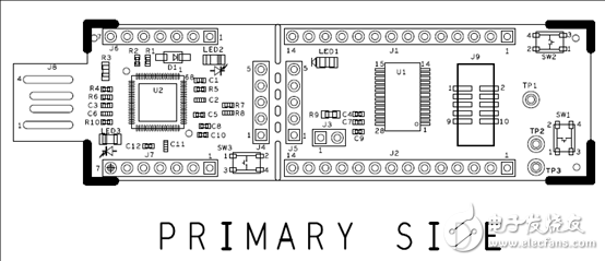
图2.原型板CY8CKIT-146PSoC 4200DS外形图

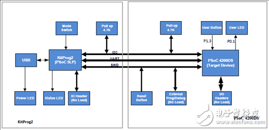
图3.原型板CY8CKIT-146PSoC 4200DS框图
图3中框图说明:
■ Reset Button:
This button is used to reset the PSoC 4200DS device when pressed.
■ Power LED: The Amber Power LED turns ON when the kits is powered from USB finger connector.
■ PSoC 4200DS Device: This is the target device on the board.
■ 10-pin Programming Header: This header allows you to program/debug the PSoC 4200DSusing an external programmer such as MiniProg3. This header is not populated by default.
■ 5-pin Programming Header: These programming headers allow you to program/debug thePSoC 4200DS using external programmers such as MiniProg3 or KitProg2. After the board issnapped, J5 can be used to program/debug the PSoC 4200DS using external programmers. J4can be used to program any other PSoC devices using the onboard PSoC 5LP (KitProg2).
■ PSoC 5LP IO Headers: These headers bring out a few GPIO lines of the onboard PSoC 5LPdevice. These include the KitProg2 USB-I2C bridge lines and USB-UART bridge lines. The additionalPSoC 5LP pins are direct connections to the internal programmable analog logic of PSoC5LP. You can use these pins as General-purpose input/output (GPIO) also.
■ Current Measurement Jumper: Using this jumper, you can measure the current consumed bythe PSoC 4200DS device. This jumper is not populated by default.
■ USB Finger Connector: A PCB USB connector is provided to connect the kit to a computer.
■ KitProg2: The CY8C5868LTI-LP039 PSoC 5LP device (U1) serving as KitProg2 is a multi-functionalsystem, which includes a programmer, debugger, USB-I2C bridge, and a USB-UARTbridge. Refer to the KitProg2 User Guide for more details.
■ KitProg2 Mode Selection Button (SW3): This button is used to switch between the KitProg2modes. You can also use this button to provide an input to the PSoC 5LP in custom applications.
Note that the switch connects the PSoC 5LP pin to ground when pressed. Table 3-1 gives a briefdescription of different LED status for various modes.
■ KitProg2 Status LED: The Amber Status LED indicates the status of KitProg2. Refer to theKitProg2 User Guide for more details.
The PSoC 4200DS Prototyping kit is simplistic in design and focuses on providing you with completeaccess to develop applications using the PSoC 4200DS device family. This kit supports the followingfeatures:
■ PSoC 4200DS I/O Headers: The PSoC 4200DS Prototyping board brings all GPIOs of the targetPSoC 4200DS device to the two expansion headers, enabling the user to have maximum accessto the capabilities of the PSoC 4200DS device.
■ User LED: The on-board LED can be used to display outputs from the PSoC 4200DS device.
This includes modulating the brightness of the LED to notify different states of the device.
■ User Button: This kit has a push button, which can be used to provide an input to the
PSoC 4200DS.
Note: The switch connects the PSoC 4200DS pin to ground when pressed. Therefore, you needto configure the PSoC 4200DS pin as ‘resistive pull-up’ for detecting the switch press.
■ Reset Button: This button is used to reset the PSoC 4200DS device when pressed.
■ Power LED: The Amber Power LED turns ON when the kits is powered from USB finger connector.
■ PSoC 4200DS Device: This is the target device on the board.
■ 10-pin Programming Header: This header allows you to program/debug the PSoC 4200DSusing an external programmer such as MiniProg3. This header is not populated by default.
■ 5-pin Programming Header: These programming headers allow you to program/debug thePSoC 4200DS using external programmers such as MiniProg3 or KitProg2. After the board issnapped, J5 can be used to program/debug the PSoC 4200DS using external programmers. J4
can be used to program any other PSoC devices using the onboard PSoC 5LP (KitProg2).
■ PSoC 5LP IO Headers: These headers bring out a few GPIO lines of the onboard PSoC 5LPdevice. These include the KitProg2 USB-I2C bridge lines and USB-UART bridge lines. The additionalPSoC 5LP pins are direct connections to the internal programmable analog logic of PSoC5LP. You can use these pins as General-purpose input/output (GPIO) also.
■ Current Measurement Jumper: Using this jumper, you can measure the current consumed bythe PSoC 4200DS device. This jumper is not populated by default.
■ USB Finger Connector: A PCB USB connector is provided to connect the kit to a computer.
■ KitProg2: The CY8C5868LTI-LP039 PSoC 5LP device (U1) serving as KitProg2 is a multi-functionalsystem, which includes a programmer, debugger, USB-I2C bridge, and a USB-UART
bridge. Refer to the KitProg2 User Guide for more details.
■ KitProg2 Mode Selection Button (SW3): This button is used to switch between the KitProg2modes. You can also use this button to provide an input to the PSoC 5LP in custom applications.
Note that the switch connects the PSoC 5LP pin to ground when pressed. Table 3-1 gives a briefdescription of different LED status for various modes. Refer to the KitProg2 User Guide for moredetails.
■ KitProg2 Status LED: The Amber Status LED indicates the status of KitProg2. Refer to theKitProg2 User Guide for more details.

图4.原型板CY8CKIT-146PSoC 4200DS电路图(1)

图5.原型板CY8CKIT-146PSoC 4200DS电路图(2)

图6.原型板CY8CKIT-146PSoC 4200DS电路图(3)

图7.原型板CY8CKIT-146PSoC 4200DS PCB设计图(1)

图8.原型板CY8CKIT-146PSoC 4200DS PCB设计图(2)

图9.原型板CY8CKIT-146PSoC 4200DS PCB设计图(3)

图10.原型板CY8CKIT-146PSoC 4200DS PCB设计图(4)

图11.原型板CY8CKIT-146PSoC 4200DS PCB设计图(5)

图12.原型板CY8CKIT-146PSoC 4200DS PCB设计图(6)

图13.原型板CY8CKIT-146PSoC 4200DS PCB设计图(7)

图14.原型板CY8CKIT-146PSoC 4200DS PCB设计图(8)

图15.原型板CY8CKIT-146PSoC 4200DS PCB设计图(9):顶层装配图

图16.原型板CY8CKIT-146PSoC 4200DS PCB设计图(10):底层装配图
原型板CY8CKIT-146PSoC 4200DS材料清单见:
CY8CKIT-146 PCBA BOM.xls
- 相关推荐
- 热点推荐
- Cypress
-
Cypress PSoC蓝牙低功耗开发方案与电路图详解2015-04-29 7210
-
大联大品佳集团推出基于Infineon产品的低成本汽车照明通用单片机解决方案2021-11-04 2574
-
Cypress PSoC蓝牙低功耗开发设计攻略2015-05-08 4392
-
CyPress是否有一个UBWebCAM参考设计解决方案?2019-04-02 1246
-
基于PSoC 4200的CY8CKIT-042,PSoC 4 Pioneer套件开发平台2019-04-10 1914
-
频率高达6GHz的可配置RF测试平台2019-06-28 2172
-
PSoC 4100与PSoC 4200的区别是什么?2019-09-11 1268
-
PSoC Creator IDE的编译器是cypress与K2010-03-04 1536
-
Mouser备货Cypress PSoC 4可编程SoC2013-06-13 1302
-
赛普拉斯半导体CY8CKIT-146 PSoC4200D原型开发套件2018-03-09 2066
-
Cypress PSoC5 架构介绍2018-06-26 5807
-
可升级和可配置的PSoC62系列MCU平台架构2019-05-01 1872
-
Cypress TrueTouch电容触摸屏的通讯接口设计方案2019-01-28 4139
-
Cypress PSoC®5开发板特性_电路图及PCB元件布局图2019-07-13 1863
-
国产混合信号处理的重要突破:浅析PSOC 7020的可配置运算架构2025-12-04 586
全部0条评论

快来发表一下你的评论吧 !

