

TI LMZM33606 6A DC/DC转换器解决方案
嵌入式技术
描述
TI公司的LMZM33606是3.5V-36V输入1V-20V输出 6A功率模块,包含了6A DC/DC转换器和功率MOSFET,屏蔽电感和小型封装的无源元件.外接元件仅需要四个,设计过程不需要回路补偿和选择电感元件. 85℃时输出功率高达50W,功率结温–40℃ 到 +125℃,主要用在工业,医疗和测试设备,通用宽VIN稳压器以及反向输出应用.本文介绍了LMZM33606主要特性,功能框图,应用电路以及评估模块LMZM33606 EVM主要特性,电路图,材料清单和PCB设计图.
The LMZM33606 power module is an easy-to-useintegrated power solution that combines a 6-A DC/DCconverter with power MOSFETs, a shielded inductor,and passives in a low-profile package. This powersolution requires as few as four external componentsand eliminates the loop compensation and inductorpart selection from the design process.
The 16 mm × 10 mm × 4 mm, 41-pin, QFN packageis easy to solder onto a printed circuit board andallows a compact, low-profile point-of-load design.
The LMZM33606 feature set includes power good,adjustable soft start, tracking, synchronization,programmable UVLO, prebias start-up, selectableauto or FPWM modes, as well as over-current andover-temperature protection. The LMZM33606 can beconfigured as negative output voltage for invertingapplications.
The LMZM33606 is a full-featured 36-V input, 6-A, synchronous step-down converter with controller, MOSFETs,shielded inductor, and control circuitry integrated into a low-profile, overmolded package. The device integrationenables small designs, while providing the ability to adjust key parameters to meet specific design requirements.
The LMZM33606 provides an output voltage range of 1 V to 20 V. An external resistor divider is used to adjustthe output voltage to the desired value. The switching frequency can also be adjusted, by either an externalresistor or a sync signal, which allows the LMZM33606 to optimize efficiency for a wide variety of input andoutput voltage conditions. The device provides accurate voltage regulation over a wide load range by using a precision internal voltage reference. The EN pin can be pulled low to put the device into standby mode to reduceinput quiescent current. The system undervoltage lockout can be adjusted using a resistor divider on the EN pin.
A power-good signal is provided to indicate when the output is within its nominal voltage range. Thermalshutdown and current limit features protect the device during an overload condition. A 41-pin, QFN package thatincludes exposed bottom pads provides a thermally enhanced solution for space-constrained applications.
LMZM33606主要特性:
1• Small Complete Solution Size: < 250 mm2
– Requires as few as 4 External Components
– 16 mm × 10 mm × 4 mm QFN Package
• Supports 5-V, 12-V, 24-V, 28-V Input Rails
– 1-V to 20-V Output Voltage Range
– Pin Compatible with 4-A LMZM33604
• Meets EN55011 Radiated Emissions
• Configurable as Negative Output Voltage
• Adjustable Features for Design Flexibility
– Switching Frequency (350 kHz to 2.2 MHz)
– Synchronization to an External Clock
– Selectable Auto Mode or FPWM Mode
– Auto: Boost Efficiency at Light Loads
– FPWM: Fixed Frequency Over Entire Load
– Adjustable Soft Start and Tracking Input
– Precision Enable to Program System UVLO
• Protection Features
– Hiccup Mode Current Limit
– Overtemperature Protection
– Power-Good Output
• Operate in Rugged Environments
– Up to 50-W Output Power at 85℃, No Airflow
– Operating Junction Range: –40℃ to +125℃
– Operating Ambient Range: –40℃ to +105℃
– Shock and Vibration Tested to Mil-STD-883D
LMZM33606应用:
• Industrial, Medical and Test Equipment
• General Purpose Wide VIN Regulation
• Inverted Output Applications
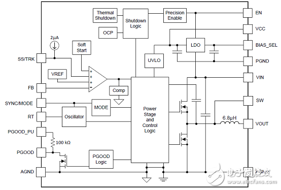
图1.LMZM33606功能框图
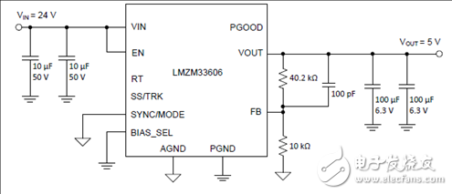
图2.LMZM33606典型应用电路图
评估模块LMZM33606 EVM
These evaluation modules (EVMs) are designed as an easy-to-use platform that facilitates an extensiveevaluation of the features and performance of the LMZM33604 and LMZM33606 power module. Thisguide provides information on the correct usage of the EVMs and an explanation of the numerous testpoints on the board.
These EVMs feature either the LMZM33604 or LMZM33606 synchronous-buck power module configuredfor operation with typical 3.5-V to 36-V input bus applications. The output voltage is set to one of fivepopular values by using a configuration jumper. Similarly, the switching frequency is set to one of fivevalues with a jumper. The EVM supplies the full output current rating of the device. Input and outputcapacitors are included on the board to accommodate the entire range of input voltage and the selectableoutput voltages on the EVM. Monitoring test points are provided to allow measurement of efficiency,power dissipation, input ripple, output ripple, line and load regulation, and transient response. Control testpoints and component footprints are provided for use of the EN, PGOOD, BIAS, and SYNC features of theLMZM33606 device. The EVMs use a recommended PCB layout that maximizes thermal performance andminimizes output ripple and noise.
图3.评估模块LMZM33606 EVM用户接口
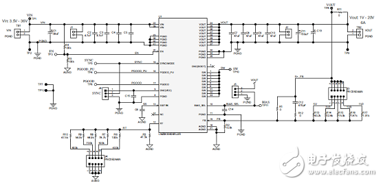
图4.评估模块LMZM33606 EVM电路图
评估模块LMZM33606 EVM材料清单:
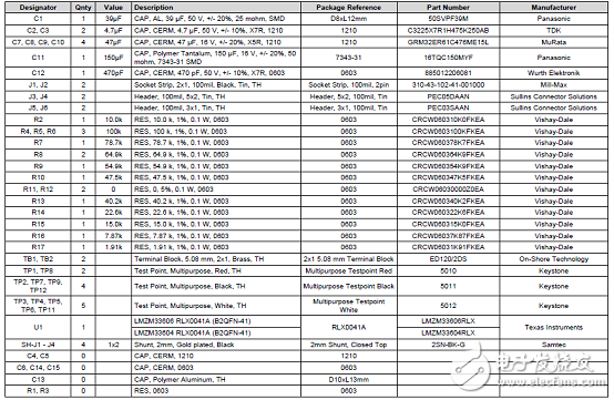

图5.评估模块LMZM33606 EVM PCB设计图(1)
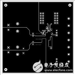
图6.评估模块LMZM33606 EVM PCB设计图(2)
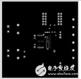
图7.评估模块LMZM33606 EVM PCB设计图(3)
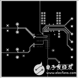
图8.评估模块LMZM33606 EVM PCB设计图(4)
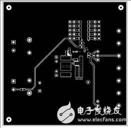
图9.评估模块LMZM33606 EVM PCB设计图(5)
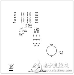
图10.评估模块LMZM33606 EVM PCB设计图(6)
- 相关推荐
- 热点推荐
- t
-
深入剖析LTC3616:6A同步降压DC/DC转换器的卓越性能与应用2026-03-11 566
-
LMZM33606电源模块:高效、灵活的电源解决方案2026-03-04 616
-
LT3154:高效6A单电感降压 - 升压DC/DC转换器的深度解析2026-03-03 1206
-
LMZM33606 3.5V 至 36V 输入、1V 至 20V 输出、6A 电源模块数据手册2025-04-21 1398
-
3.5V 至 36V 输入、1V 至 20V 输出、6A 电源模块LMZM33606数据表2024-04-28 788
-
LT3154: 6A低噪音、高性能Buck-Boost DC/DC转换器数据表 ADI2023-10-07 123
-
LTC3616:6A、4 MHz单片同步降压DC/DC转换器数据表2021-05-24 1684
-
LTC3609:32V、6A单片同步降压DC/DC转换器数据表2021-04-24 1668
-
具故障保护的 6A、2.5MHz、42V 升压/负输出 DC/DC 转换器2021-03-21 1335
-
基于Xilinx FPGA的系统的双输出DC/DC转换器解决方案2019-08-21 1874
-
TI LMZM3360x电源模块2018-10-23 2929
-
德州仪器(TI)太阳能微型转换器/DC-DC电源优化器解决方案2012-12-03 3202
-
采用TI公司DC/DC转换器的电源解决方案2010-12-11 756
-
TI推出业界最小6A、17V降压DC/DC转换器--TPS52009-07-01 1580
全部0条评论

快来发表一下你的评论吧 !
