优势和特点
- 130 MSPS guaranteed sampling rate (AD9461-130)
- 78.4 dBFS SNR with 10 MHz input
(3.4 V p-p input, 130 MSPS) - 77.1 dBFS SNR / 85 dBc SFDR with 170 MHz
input (3.4V p-p input, 130 MSPS) - 83 dBc SFDR with 225 MHz input
(3.4V p-p input, 130 MSPS) - TBD dBFS 2-tone SFDR with 170 MHz and 170 MHz (130 MSPS)
- 60 fsec rms jitter
| - Excellent linearity
DNL = ±0.6 LSB typical
INL = ±4.0 LSB typical - 2.0 V p-p to 4.0 V p-p differential full-scale input
- Buffered analog inputs
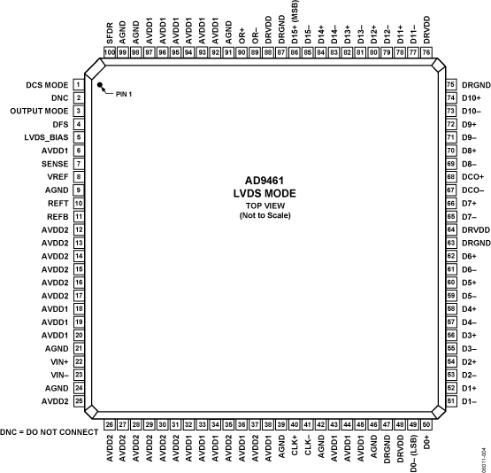
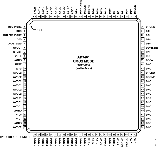
- LVDS outputs (ANSI-644 compatible) or CMOS outputs
- Data format select (offset binary or twos complement)
- Output clock available
|
产品详情
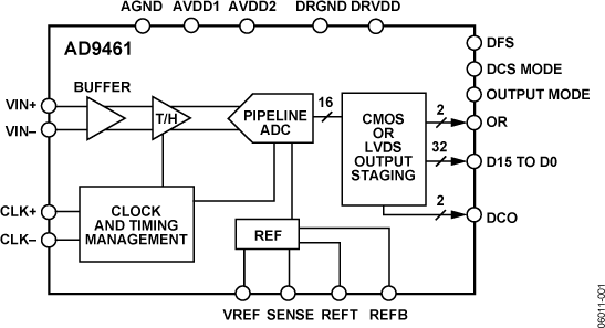
The AD9461 is a 16-bit, monolithic, sampling analog-to-digital converter (ADC) with an on-chip track-and-hold circuit. It is optimized for performance, small size, and ease of use. The product operates up to 130 MSPS, providing superior SNR for instrumentation, medical imaging, and radar receivers employing baseband (<100 MHz) and IF frequencies.
The ADC requires 3.3 V and 5.0 V power supplies and a low voltage differential input clock for full performance operation. No external reference or driver components are required for many applications. Data outputs are CMOS or LVDS compatible (ANSI-644 compatible) and include the means to reduce the overall current needed for short trace distances.
Optional features allow users to implement various selectable operating conditions, including input range, data format select, and output data mode.
The AD9461 is available in a Pb-free, 100-lead, surface-mount, plastic package (100-lead TQFP/EP) specified over the industrial temperature range −40°C to +85°C.
Product Highlights
- True 16-bit linearity.
- High performance: outstanding SNR performance for baseband IFs in data acquisition, instrumentation, magnetic resonance imaging, and radar receivers.
- Ease of use: on-chip reference and high input impedance track-and-hold with adjustable analog input range and an output clock simplifies data capture.
- Packaged in a Pb-free, 100-lead TQFP/EP package.
- Clock duty cycle stabilizer (DCS) maintains overall ADC performance over a wide range of clock pulse widths.
- OR (out-of-range) outputs indicate when the signal is beyond the selected input range.
Applications
- MRI receivers
- Multicarrier, multimode cellular receivers
- Antenna array positioning
- Power amplifier linearization
- Broadband wireless
- Radar
- Infrared imaging
- Communications instrumentation
方框图