

MAX.II的UFM模块使用实例
电子说
描述
查看MAX II器件的Chip Planner:
其左下角这块黑色区域是用户不可用资源区,而在这片不可用区域里有一块绿色的方块是可用的。这块不可用的黑色区域叫做CFM block(配置Flash存储区),而那个绿色方块叫做UFM(用户可用的Flash存储区)。对于后者是我们今天讨论的重点,先看以下官方对此存储区作用的描述:
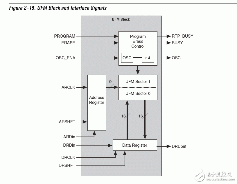
MAX II devices feature a single UFM block, which can be used like a serial EEPROM for storing non-volatile information up to 8,192 bits. The UFM block connects to the logic array through the MultiTrack interconnect,allowing any LE to interface to the UFM block. Figure 2–15 shows the UFM block and interface signals. The logic array is used to create customer interface or protocol logic to interface the UFM block data outside of the device. The UFM block offers the following features:
■ Non-volatile storage up to 16-bit wide and 8,192 total bits
■ Two sectors for partitioned sector erase
■ Built-in internal oscillator that optionally drives logic array
■ Program, erase, and busy signals
■ Auto-increment addressing
■ Serial interface to logic array with programmable interface
也就是说,MAX II其实是内嵌了一块8Kbit的Flash。这个Flash原则上是不占用MAX II的其它可用逻辑资源的,不过这有个大前提:用户读写这块存储区使用altera本身的串行接口(遵循特定的通信协议)。但是这个协议也太繁琐了(个人感觉),因此,对于这块存储区读写接口altera提供了三种通用的接口供用户选择。
■ I2C
■ SPI
■ Parallel
■ None (Altera Serial Interface)
最后一种就是不需要占用器件额外逻辑资源的接口,上面三种是需要消耗器件逻辑资源的接口。笔者添加了一个并行接口做测试,占用了EMP240内部86个LEs,对于资源比较紧张的应用还是很划不来的。
更多详细的关于UFM的信息请大家参考altera提供的MAX II datasheet。下面介绍一个使用并行接口读写UFM的实例,以及功能仿真。
新建一个工程,名为ufmtest,顶层模块ufmtest.v,代码如下:
module ufmtest(
databus,addr,
nerase,nread,nwrite,
data_valid,nbusy
);
inout[15:0] databus; //Flash数据总线
input[8:0] addr; //Flash地址总线
input nerase; //擦除Flash某一扇区信号
input nread; //读Flash信号
input nwrite; //写Flash信号
output data_valid; //Flash数据输出有效信号
output nbusy; //Flash忙信号
assign databus = nwrite ? dataout:16‘hzzzz; //写信号有效时,Flash数据总线作为输入
assign datain = databus; //写入Flash数据总线连接
wire[15:0] datain; //Flash写入数据
wire[15:0] dataout; //Flash读出数据
//例化UFM(Flash)模块
para_ufm para_ufm_inst (
.addr ( addr ),
.datain ( datain ),
.nerase ( nerase),
.nread ( nread ),
.nwrite ( nwrite),
.data_valid ( data_valid ),
.dataout ( dataout ),
.nbusy ( nbusy )
);
endmodule
但是在例化UFM模块之前,大家需要先在MegaWizard Plug-In Manager里添加一个Flash模块。步骤如下:
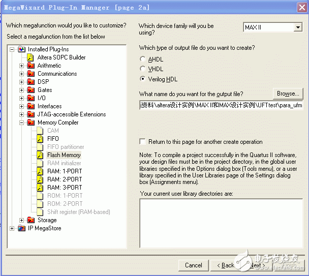
1,点击菜单栏里的ToolsàMegaWizard Plug-In Manager。弹出如下,点击next。

2,接着选择Memory Compiler下的Flash Memory,然后在What name do you want for the output file?下路径的最后添加输出文件名为para_ufm,点击next.
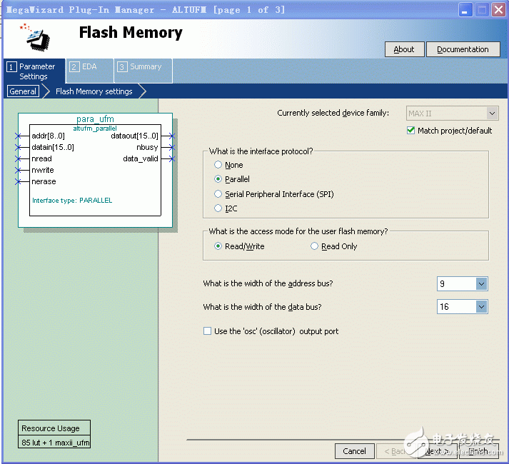
3,接下来一路Next,需要更改设置的地方如下(我也不多废话,大家一看都明白):
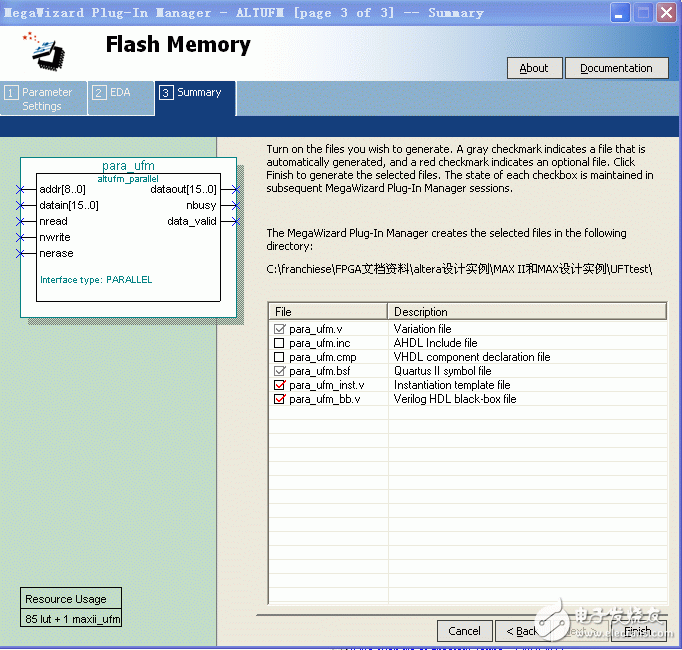
完成上面步骤以后编译工程,编写testbench如下:
`timescale 1ns/1ns
module tb_ufmtest();
//inout
wire[15:0] databus; //Flash数据总线
//input
wire data_valid; //Flash数据输出有效信号
wire nbusy; //Flash忙信号
//output
reg[8:0] addr; //Flash地址总线
reg nerase; //擦除Flash某一扇区信号
reg nread; //读Flash信号
reg nwrite; //写Flash信号
reg[15:0] databus_r; //测试模块数据总线寄存器
reg[15:0] rdback_data; //测试模块数据总线数据回读寄存器
assign databus = nwrite ? 16’hzzzz:databus_r;
ufmtest ufmtest(
.databus(databus),
.addr(addr),
.nerase(nerase),
.nread(nread),
.nwrite(nwrite),
.data_valid(data_valid),
.nbusy(nbusy)
);
parameter DELAY_600US = 600_000, //600us延时
DELAY_2US = 2_000, //2us延时
DELAY_5US = 5_000; //5us延时
initial begin
nerase = 1;
nread = 1;
nwrite = 1;
addr = 0;
databus_r = 0;
#DELAY_600US; //0地址写入数据99
databus_r = 99;
addr = 9‘d0;
nwrite = 0;
#DELAY_5US;
nwrite = 1;
@ (posedge nbusy);
#DELAY_5US; //0地址读出数据,保存到寄存器rdback_data中
databus_r = 16’hff;
addr = 9‘d0;
nread = 0;
#DELAY_5US;
nread = 1;
@ (posedge data_valid);
rdback_data = databus;
#DELAY_600US;
$stop;
end
endmodule
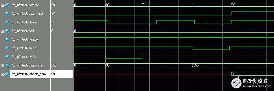
仿真波形如下:
- 相关推荐
- 热点推荐
- 模块
-
#硬声创作季 #FPGA 玩转FPGA-19 BJ-EPM240实验12-MAX II的UFM模块使用实例-1水管工 2022-10-29
-
MAX II设备系列数据2022-09-29 454
-
深入浅出玩转FPGA视频:MAX II的UFM模块使用实例2019-12-18 3934
-
FPGA视频教程:BJ-EPM240学习板-MAX II的UFM模块使用实验2019-12-11 9103
-
MAX II的UFM模块使用实例2019-11-15 2725
-
FPGA视频教程之MAX.II内部震荡时钟的使用实例详细资料说明2019-03-05 1302
-
基于VHDL的FPGA和Nios_II实例精炼2016-07-14 1402
-
MAX+Plus ii 软件2013-11-19 2262
-
max2的ufm怎么用2013-10-27 9526
-
关于MAX II上电和复位的讨论2012-05-16 2318
-
基于VHDL的FPGA与NIOS_II实例精炼代码实例下载2012-02-06 3958
-
让没有晶振的生活成为可能——UFM2012-01-17 11033
-
MAX PLUS II软件的学习2009-10-24 2985
全部0条评论

快来发表一下你的评论吧 !
