

Maxim MAX22513浪涌保护双路IO-Link收发器解决方案
嵌入式技术
描述
Maxim公司的MAX22513是双路低功耗IO-Link收发器,具有可选择的控制接口,内部高效率DC/DC降压稳压器,两个线性稳压器和集成了用于鲁棒通信的浪涌保护.器件还有低开态电阻驱动器(C/Q和DO/DI),可选择驱动电流限制和过流保护以降低功耗.DC/DC降压稳压器提供多达300mA负载电流和可调整输出电压(2.5V-12V).而内部线性稳压器产生5V和3.3V,提供高达50mA电流.MAX22513可通过SPI或I2C接口,灵活接口微控制器,支持全双工和半双工SPI.内部的MCLK振荡器为IO-LINK通信的微控制器提供时钟源.工作温度-40℃到 +125℃,主要用在IO-Link传感器和执行机构装置以及工业传感器.本文介绍了MAX22513主要优势和特性,框图和I2C接口应用电路图,半双工SPI接口应用电路图以及评估板MAX22513 EVK主要特性,框图,电路图,材料清单和PCB设计图.
The MAX22513 dual-channel low power IO-Link device transceiver features a selectable control interface, internal high-efficiency DC-DC buck regulator, two internal linear regulators, and integrated surge protection for robust communication. The device features low-on resistance drivers (C/Q and DO/DI), selectable driver current limits, and overcurrent protection to reduce power dissipation in small sensor applications.
The DC-DC buck regulator supplies up to 300mA load current and has an adjustable output voltage (from 2.5V to 12V). Internal linear regulators generate 5V and 3.3V, supplying up to 50mA of current.
The MAX22513 can be controlled using SPI or I2C interfaces, providing flexibility for microcontrollers, and extensive control and diagnostic features. Both full-and half-duplex SPI are supported. The internal MCLK oscillator provides a clock source to a microcontroller for IO-Link communication.
The MAX22513 features extensive integrated protection to ensure robust communication in harsh industrial environments. All four IO pins (V24, C/Q, DO/DI, and GND), are reverse voltage protected, short circuit protected, and feature integrated ±1kV/500Ω surge protection.
The MAX22513 is available in a tiny WLP package (4.1mm x 2.1mm) or 28-pin TQFN-EP package (3.5mm x 5.5mm) and operates over the -40℃ to +125℃ temperature range.
MAX22513主要优势和特性:
High Configurability and Integration Reduces SKU Configurable C/Q and DO/DI Drivers PNP, NPN, and Push-Pull Modes
Individual Slew Rate Control for Drivers
Selectable Driver Current Limit: 50mA to 250mA
Control and Monitoring with I2C or SPI Half- and Full-Duplex SPI Modes
Integrated High-Efficiency DC-DC Buck Regulator Selectable Switching Frequency 921kHz (typ) or 1.229MHz (typ)
300mA (max) Load
Output Voltage from 2.5V to 12V
Internal 5V and 3.3V Linear Regulators
Accurate Oscillator for IO-Link Communication
Integrated Protection Enables Robust Systems Integrated ±1kV/500Ω Surge Protection
Glitch Filters for Improved Burst Resilience
Selectable Overcurrent Configuration
Hot-Plug and Reverse Polarity Protection
-40℃ to +125℃ Operating Temperature Range
Optimized for Small Sensor Designs Low Power Dissipation: 2Ω (typ) On-Resistance for C/Q and DO/DI Drivers
Available in Two Tiny Packages: 28-Pin TQFN-EP (3.5mm x 5.5mm)
WLP (4.1mm x 2.1mm)
MAX22513应用:
IO-Link Sensor and Actuator Devices
Industrial Sensors

图1.MAX22513框图

图2. MAX22513 I2C接口应用电路图
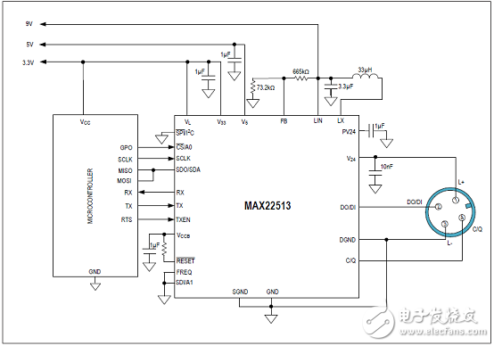
图3.9V/150mA DC/DC输出(12V最小输入)MAX22513 I2C半双工SPI接口应用电路图
评估板MAX22513 EVK
The MAX22513 evaluation kit (EV kit) consists of the evaluation board and software. The EV kit is a fully assembled and tested circuit board that evaluates the MAX22513 IO-Link® device transceiver with integrated DC-DC buck regulators.
The EV kit includes Windows®-compatible software that provides a graphical user interface (GUI) for exercising the features of the MAX22513. The EV kit is connected to a PC through a USB-A-to-micro-B cable.
评估板MAX22513 EVK主要特性:
IO-Link-Compliant Device Transceiver
I/O, I2C, and SPI Interface Terminals
Arduino® Compatible Connector
Windows 10-Compatible Software
USB-PC Connection
Proven PCB Layout
Fully Assembled and Tested

图4.评估板MAX22513 EVK框图

图5.评估板MAX22513 EVK外形图

图6.评估板MAX22513 EVK电路图
评估板MAX22513 EVK材料清单:

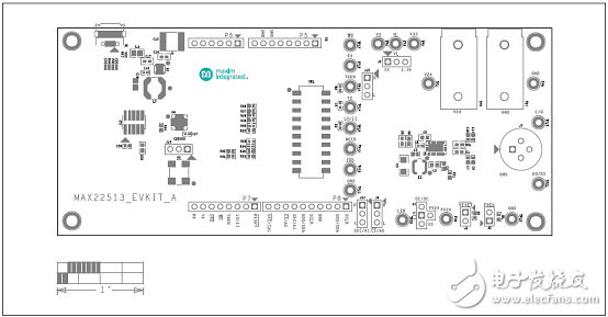
图7.评估板MAX22513 EVK PCB设计图:顶层丝印

图8.评估板MAX22513 EVK PCB设计图:顶层布局
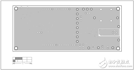
图9.评估板MAX22513 EVK PCB设计图:地层

图10.评估板MAX22513 EVK PCB设计图:电源层

图11.评估板MAX22513 EVK PCB设计图:底层布局

图12.评估板MAX22513 EVK PCB设计图:底层丝印
- 相关推荐
- 热点推荐
- Maxim
-
Maxim推出业界尺寸最小、功耗最低的智能执行器,有效提高工厂生产力2020-11-27 1278
-
IO-Link 节点简化应用设计2018-07-13 3369
-
Mouser备货业界最小的IO-Link设备收发器Maxim MAX148272016-03-28 1003
-
Maxim最新双通道收发器被Omron采纳,有效降低IO-Link传感器维护成本2017-07-28 1976
-
MAX14827 IO-Link设备收发器的FLIR热图比较2018-10-09 4442
-
MAX14819双通道IO-Link主机收发器的特点与应用2018-10-08 6459
-
Maxim推出IO-Link®设备收发器 是工业4.0应用的理想选择2019-05-16 4675
-
业界最小的IO-Link设备收发器Maxim MAX148272020-03-26 1389
-
让您的大电流传感器引领IO-Link革命2022-12-22 1680
-
计算MAX14819双通道IO-Link主收发器的功耗2023-01-13 2726
-
IO-Link收发器怎么数据读取2025-02-02 1719
-
Analog Devices Inc. MAX22516 IO-Link数据链路控制器数据手册2025-06-06 1258
-
Analog Devices / Maxim Integrated MAX22514浪涌保护IO-Link收发器数据手册2025-06-23 1177
-
具有集成浪涌保护功能的TIOL111、TIOL111x IO-Link器件收发器:功能与应用解析2025-12-18 992
-
MAX14829:低功耗IO-Link设备收发器的卓越之选2026-03-29 513
全部0条评论

快来发表一下你的评论吧 !
