

ADI AD92135G多频段无线通信RF转换器解决方案
电子说
描述
ADI公司的AD9213是12位10.25 GSPS RF模拟数转换器(ADC),输入带宽6.5GHz,支持需要宽瞬态带宽和低代码误差速率(CER)的高动态范围频率和时域应用.AD9213具有16路JESD204B接口,以支持它的最大带宽功能。它具有业界一流的动态范围和线性信性能而功耗仅为5.1W(10GSPS取样),基于交错管道架构,具有专有校准和随机化技术,它能抑制交错杂散信号进固有噪声电平。噪音频谱密度为154 dBFS/Hz, SFDR为70 dBc (1 GHz, −1 dBFS)。器件集成的输入缓冲器输入带宽为6.5GHz,RIN=50Ω时1.4Vp-p满刻度输入,集成了数字下变换器(DDC),主要用在4G/5G 多频段无线通信基站,多标准生产测试系统和防御电子产品等 GHz 带宽应用。本文介绍了AD9213主要特性,功能框图,数字下变换器(DDC)框图以及高速评估板ADS8-V1EBZ主要特性,电路图,材料清单和PCB设计图。
The AD9213 is a single 12-bit, 10.25 GSPS, RF analog-to-digital converter (ADC) with a 6.5 GHz input bandwidth. The AD9213 has been optimized to support high dynamic range frequency and time domain applications requiring wide instantaneous bandwidth and low code error rates (CER)。 The AD9213 features a 16-lane JESD204B interface to support its maximum bandwidth capability.
The AD9213 achieves industry leading dynamic range and linearity performance while consuming only 5 W. Based on an interleaved pipeline architecture, the AD9213 features a proprietary calibration and randomization technique that suppresses interleaving spurious artifacts into its noise floor. The excellent linearity performance of the AD9213 is preserved by a combination of on-chip dithering and calibration resulting in excellent spurious free performance over a wide range of input signal conditions.
Applications requiring less instantaneous bandwidth can benefit from the on-chip digital signal processing (DSP) capability of the AD9213 that reduces the output data rate along with the number of JESD204b lanes required to support it. The DSP path includes a digital downconverter (DDC) with a 48-bit, numerically controlled oscillator (NCO) followed by an I and Q digital decimator stage allowing for selectable decimation rates that are factors of two or three. For fast frequency hopping applications, the AD9213 NCO supports up to 16-profile settings with separate trigger input allowing for wide surveillance frequency coverage but at a reduced JESD204B lane count.
The AD9213 also supports sample accurate multichip synchronization that also includes synchronization of the NCOs. The AD9213 will be offered in a 192 flip-chip ball grid array (FcBGA) package. The AD9213 is specified over a junction temperature range of −10℃ to +115℃。
AD9213主要特性:
High instantaneous dynamic range
Noise spectral density 154 dBFS/Hz
SFDR 70 dBc (1 GHz, −1 dBFS)
Low power consumption: 5.1 W at 10 GSPS
Integrated input buffer (6.5 GHz input bandwidth)
1.4 V p-p full-scale input with RIN = 50 Ω
Overvoltage protection
16-lane JESD204B output (up to 16 Gbps line rate)
Multichip sync capable with 1 sample accuracy
DDC NCO synchronization included
Fast overrange detection for efficient AGC
Integrated DDC
Selectable decimation factors
16-profile settings for fast frequency hopping
Optional on-chip PLL clock multiplier
On-chip temperature sensor
On-chip negative voltage generators
Low CER 《1e−16
12 mm × 12 mm BGA
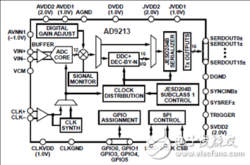
图1.AD9213功能框图
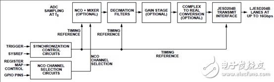
图2.AD9213数字下变换器(DDC)框图
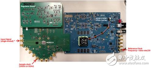
图3. AD9213评估板和ADS8-V1EBZ数据捕获板连接图
高速评估板ADS8-V1EBZ
The ADS8-V1 Evaluation Board was developed to support the evaluation of Analog Devices High Speed Data Converters with JESD204B bit rates up to 16Gbps. This Wiki site provides a high level overview of the platform. In addition, each use-case of the board has its own section (e.g. Using the ADS8-V1 for High Speed A/D Converter Evaluation)。 The ADS8-V1 is intended to be used only with specified Analog Devices Evaluation Boards. The ADS8-V1 is not intended to be used as a general purpose development platform, and no support is available for standalone operation. The ADS8-V1 may contain hardware features not fully productized or supported by our default customer evaluation configurations. Please refer to Xilinx and its approved distributors for general purpose FPGA Development Kits.
高速评估板ADS8-V1EBZ主要特性:
1. Xilinx KintexUltrascale XCKU040-3FFVA1156E FPGA.
2. One (1) FMC+ connector.
3. Twenty (20) 16Gbps transceivers supported by one (1) FMC+ connector.
4. DDR4 SDRAM.
5. Simple USB 3.0 port interface.
图4.高速评估板ADS8-V1EBZ外形图(顶面)
图5.高速评估板ADS8-V1EBZ外形图(底面)
When connected to a specified Analog Devices high speed adc evaluation board, the ADS8-V1 works as a data acquistion board. Designed to support the highest speed JESD204B A/D Converters, the FPGA on the ADS8-V1 acts as the data receiver, while the ADC is the data transmitter. A typical test setup is shown below.
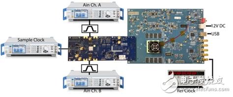
图6.高速评估板ADS8-V1EBZ和高速ADC评估板连接图
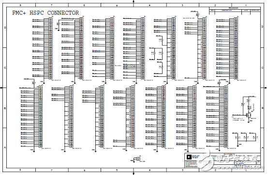
图7.高速评估板ADS8-V1EBZ电路图(1)
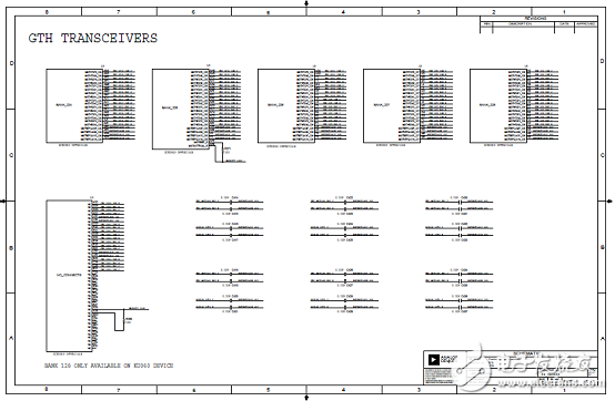
图8.高速评估板ADS8-V1EBZ电路图(2)
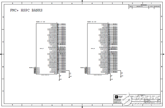
图9.高速评估板ADS8-V1EBZ电路图(3)
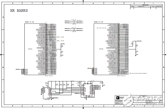
图10.高速评估板ADS8-V1EBZ电路图(4)
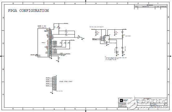
图11.高速评估板ADS8-V1EBZ电路图(5)
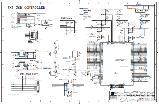
图12.高速评估板ADS8-V1EBZ电路图(6)
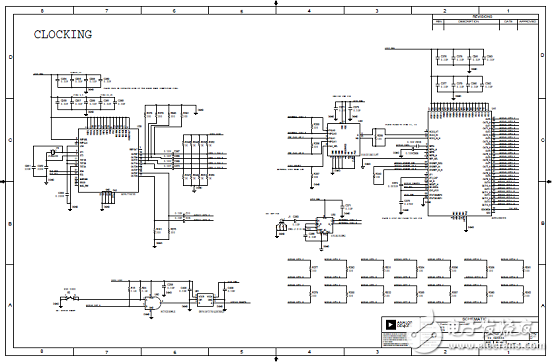
图13.高速评估板ADS8-V1EBZ电路图(7)
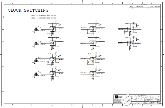
图14.高速评估板ADS8-V1EBZ电路图(8)
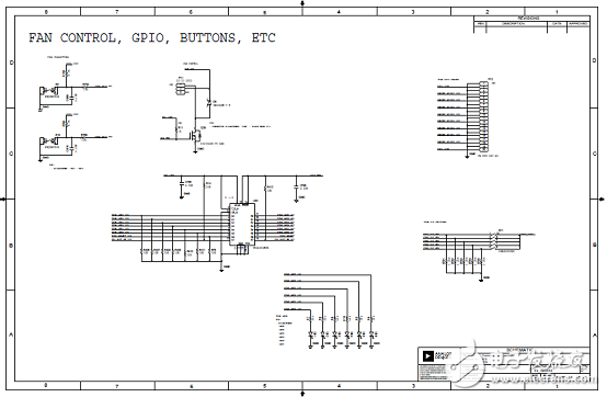
图15.高速评估板ADS8-V1EBZ电路图(9)
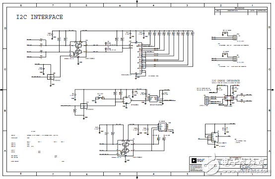
图16.高速评估板ADS8-V1EBZ电路图(10)
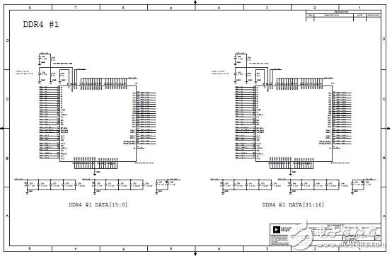
图17.高速评估板ADS8-V1EBZ电路图(11)

图18.高速评估板ADS8-V1EBZ电路图(12)
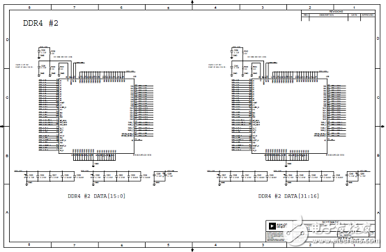
图19.高速评估板ADS8-V1EBZ电路图(13)
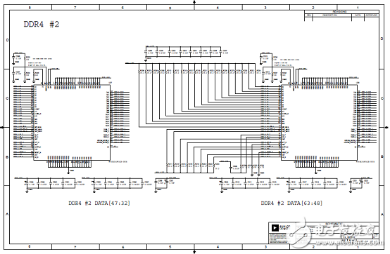
图20.高速评估板ADS8-V1EBZ电路图(14)
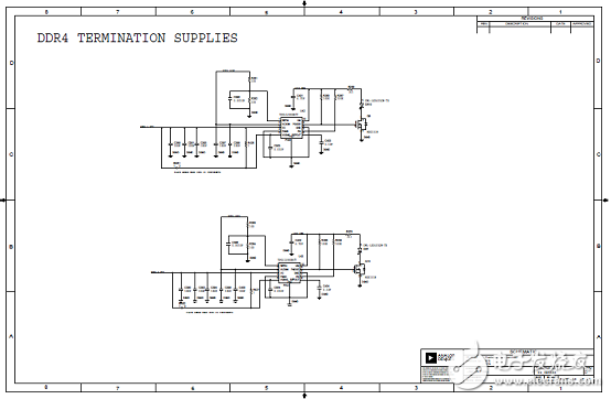
图21.高速评估板ADS8-V1EBZ电路图(15)
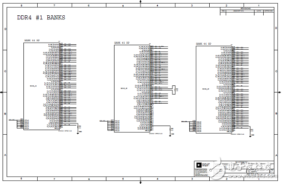
图22.高速评估板ADS8-V1EBZ电路图(16)
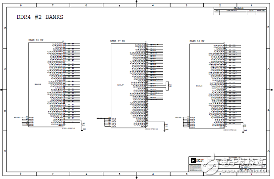
图23.高速评估板ADS8-V1EBZ电路图(17)
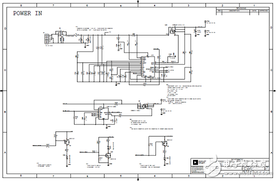
图24.高速评估板ADS8-V1EBZ电路图(18)
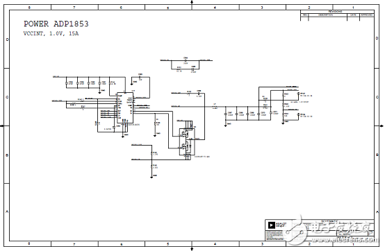
图25.高速评估板ADS8-V1EBZ电路图(19)
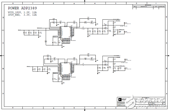
图26.高速评估板ADS8-V1EBZ电路图(20)
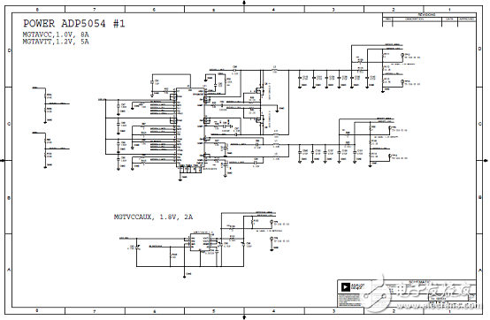
图27.高速评估板ADS8-V1EBZ电路图(21)
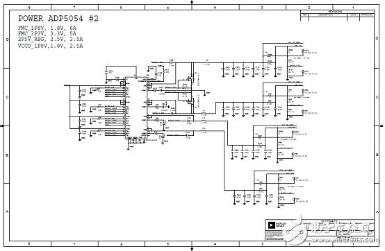
图28.高速评估板ADS8-V1EBZ电路图(22)
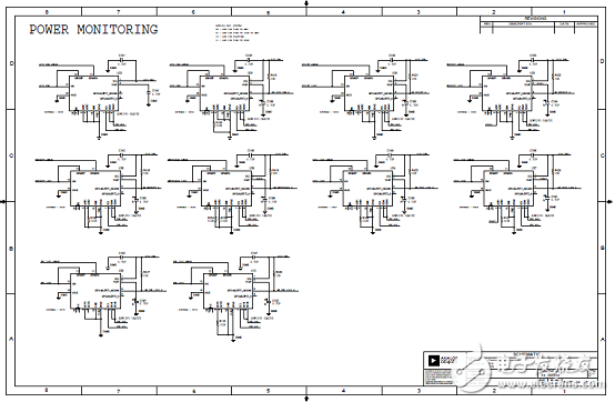
图29.高速评估板ADS8-V1EBZ电路图(23)
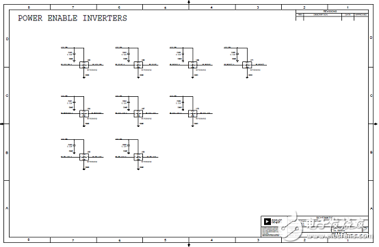
图30.高速评估板ADS8-V1EBZ电路图(24)
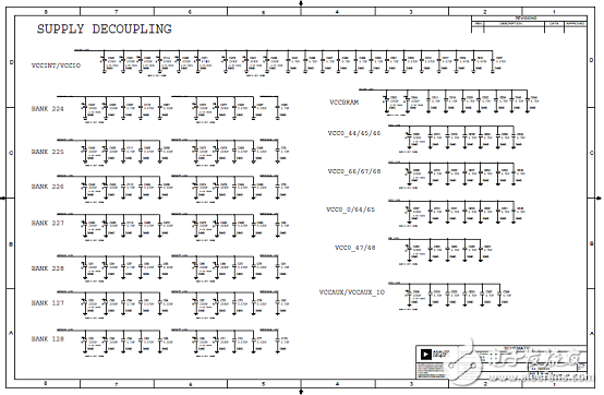
图31.高速评估板ADS8-V1EBZ电路图(25)
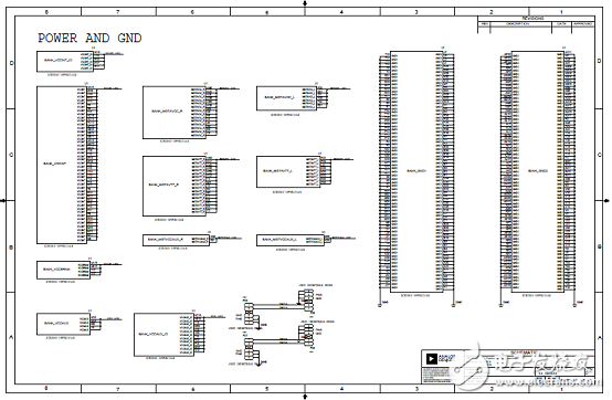
图32.高速评估板ADS8-V1EBZ电路图(26)
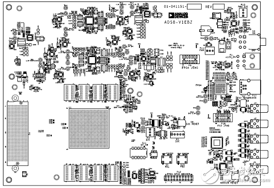
图33.高速评估板ADS8-V1EBZ PCB设计图(1)
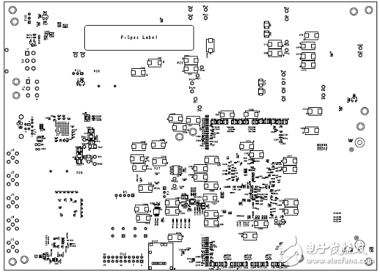
图34.高速评估板ADS8-V1EBZ PCB设计图(2)
-
ADI 最新中文资料2018-07-30 3658
-
转换器简化RF信号链-汽车收音机的演变历程2018-08-03 2030
-
高速转换器的创新从三个方面改变世界2018-10-11 1456
-
RF转换器,兑现提供真正宽带无线电的承诺2018-10-25 2449
-
高速转换器如何简化RF信号链?2018-10-31 1829
-
RF数模转换器在通信领域有什么应用?2019-08-14 3519
-
RF DAC多频带发射器线性性能怎么评估?2019-10-23 2257
-
一个针对多频段应用的直接RF发射机例子2021-07-23 5298
-
ZigBee无线通信的频段是什么意思2021-09-24 3629
-
支持宽带无线电的技术之RF转换器2022-01-04 6685
-
瑞萨电子将与AMD合作5G有源天线系统无线电RF前端解决方案2023-02-21 1125
-
采用RFDAC的多频段、多标准发射器设计2017-11-16 3578
-
利用ADI RF转换器打造一个带DPD接收机的直接RF发射机2019-12-17 2679
-
ADI无线通信技术解决方案全方位覆盖2020-10-26 4251
-
RF转换器为下一代无线基站提供多频段无线电2023-11-23 525
全部0条评论

快来发表一下你的评论吧 !
