

我们是AGM的长期授权代理商,可以为用户提供最具竞争力的价格与技术支持服务。
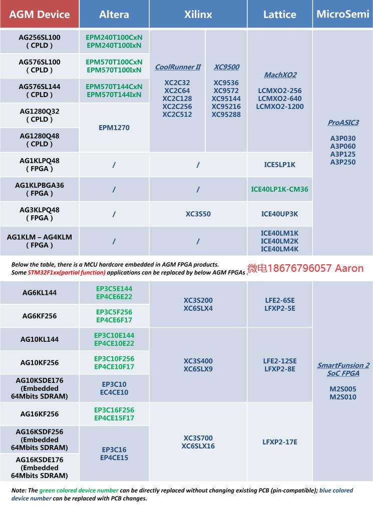
功能替换 Altera Xilinx Lattice MicroSemi FPGA:
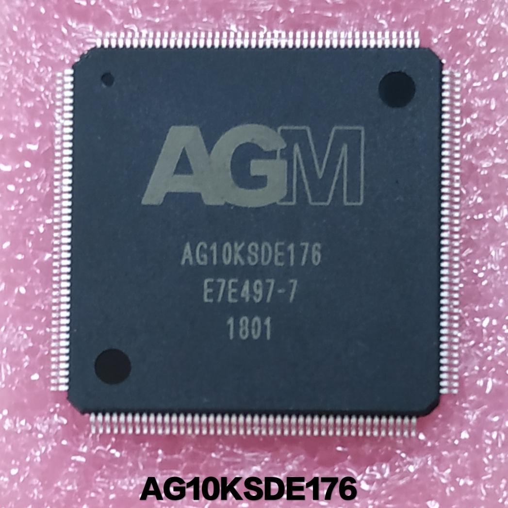
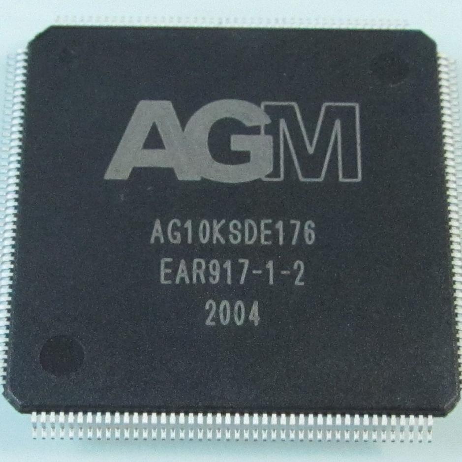
AG10KSDE176
Altera:EP3C10 EP4CE10
Xilinx:XC3S400 XC6SLX9
Lattice:LFXP2-8E LFE2-12SE
MicroSemi:M2S005 M2S010
AG10K(+MCU) SoC AG10KSDE176
可以替代部分STM32F1XX的应用功能
FPGA+MCU SoC family device, integrates high performance FPGA logic with low-power MCU core in a single die one silicon, targets consumer and industrial's mass-volume market with low-cost and high-performance SoC. The device features integrated rich functions with 16K LUTs and MCU core with 250MHz.
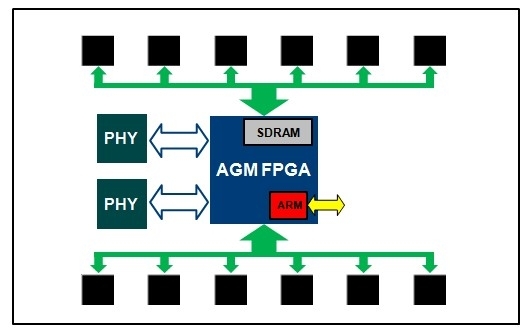
MCU hard-IP is embedded within FPGA logic fabric, and all mcu internal IOs are connectable to device's IO pad, and/or internal FPGA's logic as user demands. Cortex MCU, with usable code space up to 64 KByte RAM, is programmable through spiflash, and JTAG for testing purposes. Additionally,
Features
High-density architecture with 10K LEs
M9K embedded memory blocks, up to 414Kbits of RAM space
Up to 23 18 x 18-bit embedded multipliers are each configurable as two independent 9 x 9-bit multipliers
Provides 2 PLLs per device provide clock multiplication and phase shifting
High-speed differential I/O standard support, including LVDS, RSDS, mini-LVDS, LVPECL
Single-ended I/O standard support, including 3.3V, 2.5V, 1.8V, and 1.5V LVCMOS and LVTTL
General package options, LQFP-144, -176 and FBGA-256
Flexible device configuration through JTAG and SPI interface
Support remote update, by "dual-boot" like implementation
Packaging types include BGA256, and QFP144.
AG10KSDE176(+MCU)+SDRAM device is AG10KSDE176(+MCU) SoC bonded with 64MBit 32-bit 166MHz SDRAM die. EQFP-176 package is provided as industrial grade, is pin-to-pin compatible with AG16KSDE176(+MCU)+SDRAM.
MCU hard-IP is embedded within FPGA logic fabric, and all mcu internal IOs are connectable to device's IO pad, and/or internal FPGA's logic as user demands. MCU core, with usable code space up to 64 KByte RAM, is programmable through spiflash, and JTAG for testing purposes.
AGM(遨格芯)2012年起步于仅是 FPGA IP 软核和软件授权公司, 2014年转入芯片业务,CPLD芯片已经成熟,并且开始在行业有了一些应用,看到智能手机风口的AGM也不失时机出了一款用于智能手机和loT的FPGA芯片,并且通过了三星严格的供应商测试认证,成为三星Galaxy手机里除Lattice之外的唯一备选FPGA器件,实现了国内FPGA公司出口零的突破,具有特殊的战略意义。
AGM在软件和电路上拥有自主知识产权,在产品方面目前走的是兼容主流大厂并软硬件生态不变的路线,在芯片内部接口兼容主流厂商器件,PCB板级可以直接替换并用AGM编译软件导入烧写,AGM目前供货器件可以直接替换:
CPLD系列,针对Altera MAX II系列,包括EPM240T100,EPM570T144,EPM570T100
低端FPGA SoC系列,针对Altera Cyclone III 系列FPGA:EP3C5E、EP3C5F、EP3C10E、EP3C10F、EP3C16F; Cyclone IV 系列FPGA:EP4CE6、EP4CE10、EP4CE15
高端FPGA SoC系列BlueWind,针对Xilinx Virtex系列。
以下是替代列表:
绿色料号,直接PINtoPIN,不需要重新画板、打板,也不需要重新编程。
包装规格:
