ONFI I/O
ONFI I/O is a non-volatile memory interface technology with high bandwidth capabilities, mainly developed for flash storage applications. M31 provides a silicon-proven ONFI I/O in a variety of process nodes, which complies with international Open NAND Flash Interface specification, providing on-die termination (ODT) and supporting ZQ impedance calibration, and can be customized based on customer specifications. The ONFI 6.0, ONFI 5.1, and ONFI 5.0 I/O IP have been silicon-proven at advanced FinFet nodes. In addition, M31 also provides solutions for signal integrity (SI) issues such as FFE and DFE.

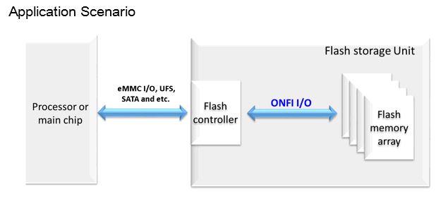
Application Scenario of ONFI I/O
Challenge of high speed ONFI
(a) TX Eye Diagram (4800Mpbs with 3.6pF @6nm, DFE off)
(b) TX Eye Diagram (4800Mpbs with 3.6pF @6nm, DFE on)
Features
- Supports ONFI 6.0(4.8Gbps), ONFI 5.1(3.6Gbps), ONFI 5.0(2.4Gbps), ONFI 4.1(1.2Gbps), ONFI 4.0(800Mbps) & ONFI 3.2(533Mbps)
- Power-sequence free
- Provides multi-driving-strength selection
- Provides CTT mode and LTT mode
- Provides two receivers (Schmitt trigger and LVCMOS receiver) in a cell, which can be selected by the register.
- Provides ODT (On-Die Termination)
- Provides ZQ Calibration


