| PGA/VGA | VGA |
| Number of channels (#) | 1 |
| BW @ Acl (MHz) | 35 |
| Vs (Max) (V) | 10 |
| Vs (Min) (V) | 10 |
| Acl, min spec gain (V/V) | 0.01 |
| Gain (Max) (dB) | 40 |
| Slew rate (Typ) (V/us) | 350 |
| Operating temperature range (C) | -40 to 85 |
| Features | Analog Gain Set, Differential to Single-ended conversion |
- High Gain Adjust Range: ±40 dB
- Differential In, Single-Ended Out
- Low Input Noise Voltage: 2.4 nV/√Hz
- Constant Bandwidth vs Gain: 35 MHz
- High dB/V Gain Linearity: ±0.3 dB
- Gain Control Bandwidth: 25 MHz
- Low Output DC Error: < ±40 mV
- High Output Current: &plsumn;60 mA
- Low Supply Current: 24.8 mA
(Maximum for –40°C to 85°C Temperature Range) - APPLICATIONS
- Optical Receiver Time Gain Control
- Sonar Systems
- Voltage-Tunable Active Filters
- Log Amplifiers
- Pulse Amplitude Compensation
- AGC receivers With RSSI
- Improved Replacement for VCA610
All other trademarks are the property of their respective owners
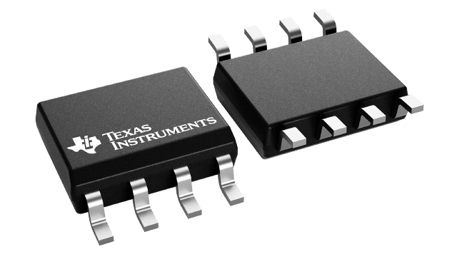
The VCA810 is a DC-coupled, wideband, continuously variable, voltage-controlled gain amplifier. The device provides a differential input to single-ended output conversion with a high-impedance gain control input used to vary the gain over a ?40-dB to 40-dB range linear in dB/V.
Operating from ±5-V supplies, the device gain control voltage adjusts the gain from ?40 dB at a 0-V input to 40 dB at a ?2-V input. Increasing the control voltage above ground attenuates the signal path to greater than 80 dB. Signal bandwidth and slew rate remain constant over the entire gain adjust range. This 40-dB/V gain control is accurate within ±1.5 dB (±0.9 dB for high grade), allowing the gain control voltage in an AGC application to be used as a received signal strength indicator (RSSI) with ±1.5-dB accuracy.
Excellent common-mode rejection and common-mode input range at the two high-impedance inputs allow the device to provide a differential receiver operation with gain adjust. The output signal is referenced to ground. Zero differential input voltage gives a 0-V output with a small DC offset error. Low input noise voltage ensures good output SNR at the highest gain settings.
In applications where pulse edge information is critical, and the device is being used to equalize varying channel loss, minimal change in group delay over gain setting retains excellent pulse edge information.
An improved output stage provides adequate output current to drive the most demanding loads. Although principally intended to drive analog-to-digital converters (ADCs) or second-stage amplifiers, the ±60-mA output current easily drives doubly-terminated 50-Ω lines or a passive post-filter stage over the ±1.7-V output voltage range.


