| Function | Zero-delay |
| Additive RMS jitter (Typ) (fs) | 120 |
| Output frequency (Max) (MHz) | 180 |
| Number of outputs | 8 |
| Output supply voltage (V) | 3.3 |
| Core supply voltage (V) | 3.3 |
| Output skew (ps) | 150 |
| Features | Spread spectrum clocking (SSC) |
| Operating temperature range (C) | -40 to 85 |
| Rating | Catalog |
| Output type | LVTTL |
| Input type | LVTTL |
- Phase-Locked Loop-Based Multiplier by Four
- Input Frequency Range: 2.5 MHz to 45 MHz
- Output Frequency Range: 10 MHz to 180 MHz
- LVCMOS/LVTT I/O Compatible
- Low Jitter (Cycle-Cycle): ±120 ps Over the Range 75 MHz to 180 MHz
- Distributes One Clock Input to Two Banks of Four Outputs
- Auto Frequency Detection to Disable Device (Power-Down Mode)
- Operates From Single 3.3-V Supply
- Industrial Temperature Range –40°C to 85°C
- 25-
 On-Chip Series Damping Resistors
 - No External RC Network Required
- Spread Spectrum Clock Compatible (SSC)
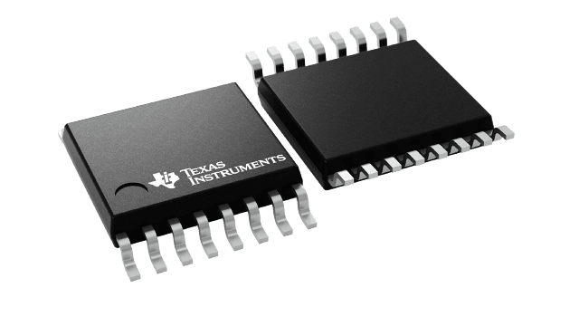
- Available in 16-Pin TSSOP Package
The CDCVF25084 is a high-performance, low-skew, low-jitter, phase-lock loop clock multiplier. It uses a PLL to precisely align, in both frequency and phase, the output clocks to the input clock signal including a multiplication factor of four. The CDCVF25084 operates from a nominal supply voltage of 3.3 V. The device also includes integrated series-damping resistors in the output drivers that make it ideal for driving point-to-point loads.
Two banks of four outputs each provide low-skew, low-jitter copies of CLKIN x four. All outputs operate at the same frequency. Output duty cycles are adjusted to 50%, independent of duty cycle at CLKIN. The device automatically goes into power-down mode when no input signal is applied to CLKIN and the outputs go into a low state. Unlike many products containing PLLs, the CDCVF25084 does not require an external RC network. The loop filter for the PLL is included on-chip, minimizing component count, space, and cost.
Because it is based on a PLL circuitry, the CDCVF25084 requires a stabilization time to achieve phase lock of the feedback signal to the reference signal. This stabilization is required following power up and application of a fixed-frequency signal at CLKIN and any following changes to the PLL reference.
The CDCVF25084 is characterized for operation from ?40°C to 85°C.


