| Function | Clock jitter cleaner, Fanout buffer |
| Number of outputs | 2 |
| Output frequency (Max) (MHz) | 683.28 |
| Core supply voltage (V) | 3.3 |
| Output supply voltage (V) | 3.3 |
| Input type | XTAL |
| Output type | LVPECL |
| Operating temperature range (C) | -40 to 85 |
| Features | I2C, Pin programmable |
| Rating | Catalog |
- Single 1.8V Supply
- High-Performance Clock Multiplier, Distributor, Jitter Cleaner, and Buffer
With 11 Outputs - Low Output Jitter: 400fs RMS
- Output Group Phase Adjustment
- Low-Voltage Differential Signaling (LVDS) Input, 100Ω Differential On-Chip
Termination, 30MHz to 319MHz Frequency Range - Differential Current Mode Logic (CML) Outputs, 50Ω Single-Ended On-Chip
Termination, 15MHz to 1.25GHz Frequency Range - One Dedicated Differential CML Output, Straight PLL and Frequency Divider Bypass
- Two Groups of Five Outputs Each with Independent Frequency Division Ratios;
Optional PLL Bypass - Fully Integrated Voltage Controlled Oscillator (VCO); Supports Wide Output
Frequency Range - Output Frequency Derived From VCO Frequency with Divide Ratios of 1, 2, 4,
5, 8, 10, 16, 20, 32, 40, and 80 - Meets OBSAI RP1 v1.0 Standard and CPRI v2.0 Requirements
- Meets ANSI TIA/EIA-644-A-2001 LVDS Standard Requirements
- Integrated LC Oscillator Allows External Bandwidth Adjustment
- PLL Lock Indication
- Power Consumption: 640mW Typical
- Output Enable Control for Each Output
- SDA/SCL Device Management Interface
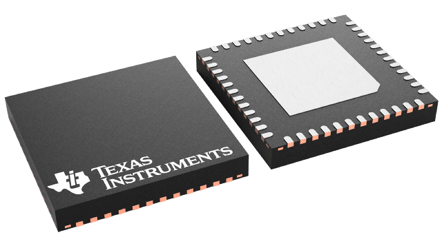
- 48-pin QFN (RGZ) Package
- Industrial Temperature Range: –40°C to +85°C
- APPLICATIONS
- Low Jitter Clocking for High-Speed SERDES
- Jitter Cleaning of SERDES Reference Clocks for 1G/10G Ethernet,
1X/2X/4X/10X Fibre Channel, PCI Express, Serial ATA, SONET, CPRI,
OBSAI, etc. - Up to 1-to-11 Clock Buffering and Fan-out
All other trademarks are the property of their respective owners.
The CDCL6010 is a high-performance, low phase noise clock multiplier, distributor, jitter cleaner, and low skew buffer. It effectively cleans a noisy system clock with a fully-integrated low noise Voltage Controlled Oscillator (VCO) that operates in the 1.2GHz?1.275GHz range. (Note that the LC oscillator oscillates in the 2.4GHz?2.55GHz range. The frequency is predivided by 2 before the post-dividers P0 and P1.)
The output frequency (FOUT) is synchronized to the frequency of the input clock (FIN). The programmable pre-dividers, M and N, and the post-dividers, P0 and P1, give a high flexibility to the ratio of the output frequency to the input frequency:
FOUT = FIN × N/(M × P)
Where:
P (P0, P1) = 1, 2, 4, 5, 8, 10, 16, 20, 32, 40, 80
M = 1, 2, 4, 8
N = 32, 40
provided that:
30MHz < (FIN /M) < 40MHz
1200MHz < (FOUT × P) < 1275MHz
The PLL loop bandwidth is user-selectable by external filter components or by using the internal loop filter. The PLL loop bandwidth and damping factor can be adjusted to meet different system requirements.
The CDCL6010 supports one differential LVDS clock input and a total of 11 differential CML outputs. One output is a straight bypass with no support for jitter cleaning or clock multiplication. The remaining 10 outputs are available in two groups of five outputs each with independent frequency division ratios. Those 10 outputs can be optionally setup to bypass the PLL when no jitter cleaning is needed. The CML outputs are compatible with LVDS receivers if ac-coupled.
With careful observation of the input voltage swing and common-mode voltage limits, the CDCL6010 can support a single-ended clock input as outlined in the Pin Description Table
The CDCL6010 can operate as a multi-output clock buffer in a PLL bypass mode.
All device settings are programmable through the SDA/SCL, serial two-wire interface.
The serial interface is 1.8V tolerant only.
The phase of one output group relative to the other can be adjusted through the SDA/SCL interface. For post-divide ratios (P0, P1) that are multiples of 5, the total number of phase adjustment steps (n) equals the divide-ratio divided by 5. For post-divide ratios (P0, P1) that are not multiples of 5, the total number of steps (n) is the same as the post-divide ratio. The phase adjustment step (
 ) in time units is given as:

 = 1/(n × FOUT)
where FOUT is the respective output frequency.
The device operates in a 1.8V supply environment and is characterized for operation from ?40°C to +85°C.
The CDCL6010 is available in a 48-pin QFN (RGZ) package.


