| Sample rate (Max) (MSPS) | 80 |
| Resolution (Bits) | 16 |
| Number of input channels | 1 |
| Interface type | Parallel CMOS, Parallel LVDS |
| Analog input BW (MHz) | 250 |
| Features | High Performance |
| Rating | Catalog |
| Input range (Vp-p) | 3.6 |
| Power consumption (Typ) (mW) | 865 |
| Architecture | Pipeline |
| SNR (dB) | 84 |
| ENOB (Bits) | 13.1 |
| SFDR (dB) | 85 |
| Operating temperature range (C) | -40 to 85 |
| Input buffer | No |
- 16-Bit Resolution
- Maximum Sample Rate:
- ADS5562: 80 MSPS
- ADS5560: 40 MSPS
- Total Power:
- 865 mW at 80 MSPS
- 674 mW at 40 MSPS
- No Missing Codes
- High SNR: 84 dBFS (3 MHz IF)
- SFDR: 85 dBc (3 MHz IF)
- Low-Frequency Noise Suppression Mode
- Programmable Fine Gain, 1-dB steps Until
6-dB Maximum Gain - Double Data-Rate (DDR) LVDS and Parallel
CMOS Output Options - Internal and External Reference Support
- 3.3-V Analog and Digital Supply
- Pin-for-Pin With ADS5547 Family
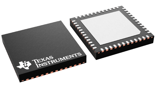
- 48-VQFN Package (7.00 mm × 7.00 mm)
The ADS556x is a high-performance 16-bit family of ADCs with sampling rates up to 80 MSPS. The device supports very-high SNR for input frequencies in the first Nyquist zone. The device includes a low-frequency noise suppression mode that improves the noise from DC to about 1 MHz.
In addition to high performance, the device offers several flexible features such as output interface (either Double Data Rate [DDR] LVDS or parallel CMOS) and fine gain in 1-dB steps until 6-dB maximum gain.
Innovative techniques, such as DDR LVDS and an internal reference that does not require external decoupling capacitors, have been used to achieve significant savings in pin count. This innovation results in a compact 7-mm × 7-mm 48-pin VQFN package.
The device can be put in an external reference mode, where the VCM pin behaves as the external reference input. For applications where power is important, the ADS556x device offers power down modes and automatic power scaling at lower sample rates.
The device is specified over the industrial temperature range of ?40°C to 85°C.


