| Sample rate (Max) (MSPS) | 65 |
| Resolution (Bits) | 10 |
| Number of input channels | 8 |
| Interface type | Serial LVDS |
| Analog input BW (MHz) | 520 |
| Features | Low Power |
| Rating | Catalog |
| Input range (Vp-p) | 2 |
| Power consumption (Typ) (mW) | 616 |
| Architecture | Pipeline |
| SNR (dB) | 61.7 |
| ENOB (Bits) | 9.94 |
| SFDR (dB) | 85 |
| Operating temperature range (C) | -40 to 85 |
| Input buffer | No |
- Speed and Resolution Grades:
- 10-bit, 65MSPS
- Power Dissipation:
- 46mW/Channel at 30MSPS
- 53mW/Channel at 40MSPS
- 62mW/Channel at 50MSPS
- 74mW/Channel at 65MSPS
- 61.7dBFS SNR at 10MHz IF
- Analog Input Full-Scale Range: 2VPP
- Low-Frequency Noise Suppression Mode
- 6dB Overload Recovery in One Clock
- External and Internal (Trimmed) Reference
- 3.3V Analog Supply, 1.8V Digital Supply
- Single-Ended or Differential Clock:
- Clock Duty Cycle Correction Circuit (DCC)
- Programmable Digital Gain: 0dB to 12dB
- Serialized DDR LVDS Output
- Programmable LVDS Current Drive, Internal Termination
- Test Patterns for Enabling Output Capture
- Straight Offset Binary or Two’s Complement Output
- Package Options:
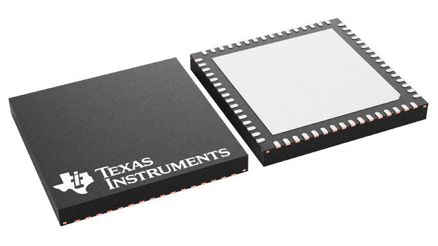
- 9mm × 9mm QFN-64
The ADS5287 is a high-performance, low-power, octal channel analog-to-digital converter (ADC). Available in a 9mm × 9mm QFN package, with serialized low-voltage differential signaling (LVDS) outputs and a wide variety of programmable features, the ADS5287 is highly customizable for a wide range of applications and offers an unprecedented level of system integration. An application note, XAPP774 (available at www.xilinx.com), describes how to interface the serial LVDS outputs of TI?s ADCs to Xilinx field-programmable gate arrays (FPGAs). The ADS5287 is specified over the industrial temperature range of –40°C to +85°C.


