| Sample rate (Max) (MSPS) | 125 |
| Resolution (Bits) | 14 |
| Number of input channels | 2 |
| Interface type | Serial LVDS |
| Analog input BW (MHz) | 500 |
| Features | High Performance |
| Rating | Catalog |
| Input range (Vp-p) | 2 |
| Power consumption (Typ) (mW) | 1000 |
| Architecture | Pipeline |
| SNR (dB) | 73.7 |
| ENOB (Bits) | 11.7 |
| SFDR (dB) | 87 |
| Operating temperature range (C) | -40 to 85 |
| Input buffer | No |
- Maximum Sample Rate: 125 MSPS
- 14-Bit Resolution with No Missing Codes
- Simultaneous Sample and Hold
- 3.5 dB Coarse Gain and up to 6 dB Programmable
Fine Gain for SFDR/SNR Trade-Off - Serialized LVDS Outputs with Programmable
Internal Termination Option - Supports Sine, LVCMOS, LVPECL, LVDS Clock Inputs
and Amplitude down to 400 mVpp - Internal Reference with External Reference
Support - No External Decoupling Required for References
- 3.3-V Analog and Digital Supply
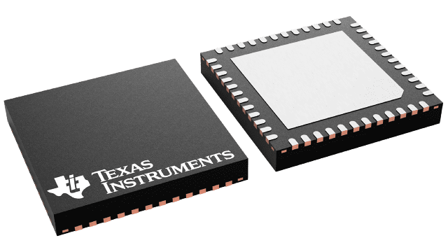
- 48 QFN Package (7 mm × 7 mm)
- Pin Compatible 12-Bit Family (ADS622X - SLAS543A)
- Feature Compatible Quad Channel Family
(ADS644X - SLAS531A and ADS642X - SLAS532A)
ADS6245/ADS6244/ADS6243/ADS6242 (ADS624X) is a family of high performance 14-bit 125/105/80/65 MSPS dual channel A-D converters. Serial LVDS data outputs reduce the number of interface lines, resulting in a compact 48-pin QFN package (7 mm × 7mm) that allows for high system integration density. The device includes 3.5 dB coarse gain option that can be used to improve SFDR performance with little degradation in SNR. In addition to the coarse gain, fine gain options also exist, programmable in 1dB steps up to 6dB.
The output interface is 2-wire, where each ADC data is serialized and output over two LVDS pairs. This makes it possible to halve the serial data rate (compared to a 1-wire interface) and restrict it to less than 1Gbps easing receiver design. The ADS624X also includes the traditional 1-wire interface that can be used at lower sampling frequencies.
An internal phase lock loop (PLL) multiplies the incoming ADC sampling clock to derive the bit clock. The bit clock is used to serialize the 14-bit data from each channel. In addition to the serial data streams, the frame and bit clocks are also transmitted as LVDS outputs.
The LVDS output buffers have features such as programmable LVDS currents, current doubling modes and internal termination options. These can be used to widen eye-openings and improve signal integrity, easing capture by the receiver.
The ADC channel outputs can be transmitted either as MSB or LSB first and 2s complement or straight binary.
ADS624X has internal references, but can also support an external reference mode. The device is specified over the industrial temperature range (–40°C to 85°C).


