| Resolution (Bits) | 12 |
| Number of DAC channels (#) | 8 |
| Interface type | SPI |
| Output type | Buffered Voltage |
| Settling time (μs) | 15 |
| Features | On-chip Offset and Gain Calibration, SDO |
| Reference type | Ext |
| Architecture | String |
| Rating | Catalog |
| Output range (Max) (mA/V) | 33 |
| Output range (Min) (mA/V) | -16.5 |
| Operating temperature range (C) | -40 to 85 |
- Bipolar Output: ±2V to ±16.5V
- Unipolar Output: 0V to +33V
- 12-Bit Resolution
- Low Power: 14.4mW/Ch (Bipolar Supply)
- Relative Accuracy: 1 LSB Max
- Low Zero/Full-Scale Error: ±1 LSB Max
- Flexible System Calibration
- Low Glitch: 4nV-s
- Settling Time: 15μs
- Channel Monitor Output
- Programmable Gain: x4/x6
- Programmable Offset
- SPI: Up to 50MHz, 1.8V/3V/5V Logic
- Schmitt Trigger Inputs
- Daisy-Chain with Sleep Mode Enhancement
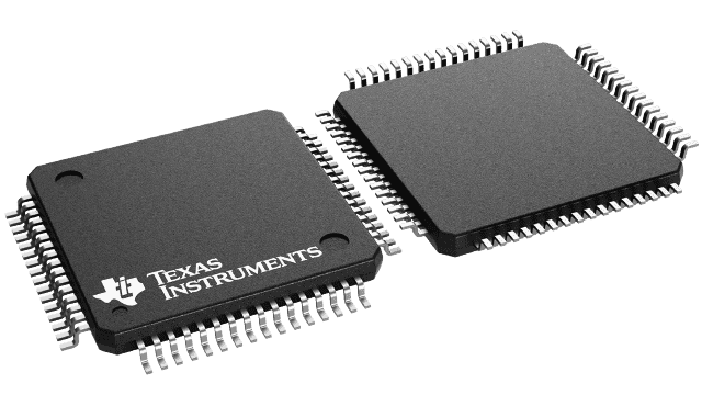
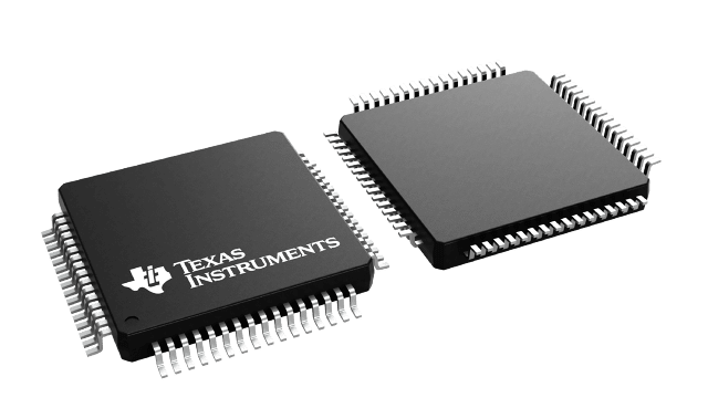
- Packages: QFN-48 (7x7mm), TQFP-64 (10x10mm)
- APPLICATIONS
- Automatic Test Equipment
- PLC and Industrial Process Control
- Communications
The DAC7718 is a low-power, octal, 12-bit digital-to-analog converter (DAC). With a 5V reference, the output can either be a bipolar ±15V voltage when operating from dual ±15.5V (or higher) power supplies, or a unipolar 0V to +30V voltage when operating from a +30.5V (or higher) power supply. With a 5.5V reference, the output can either be a bipolar ±16.5V voltage when operating from dual ±17V (or higher) power supplies, or a unipolar 0V to +33V voltage when operating from a +33.5V (or higher) power supply. This DAC provides low-power operation, good linearity, and low glitch over the specified temperature range of –40°C to +105°C. This device is trimmed in manufacturing and has very low zero-code and gain error. In addition, system level calibration can be performed over the entire signal chain. The output range can be offset by using the DAC offset register.
The DAC7718 features a standard, high-speed serial peripheral interface (SPI) that operates at up to 50MHz and is 1.8V, 3V, and 5V logic compatible, to communicate with a DSP or microprocessor. The input data of the device are double-buffered. An asynchronous load input (LDAC) transfers data from the DAC data register to the DAC latch. The asynchronous CLR input sets the output of all eight DACs to AGND. The VMON pin is a monitor output that connects to the individual analog outputs, the offset DAC, the reference buffer outputs, and two external inputs through a multiplexer (mux).
The DAC7718 is pin-to-pin and function-compatible with the DAC8718 (16-bit) and the DAC8218 (14-bit).


