| Resolution (Bits) | 12 |
| Number of DAC channels (#) | 2 |
| Interface type | Parallel CMOS |
| Sample/update rate (MSPS) | 200 |
| Features | Low Power |
| Rating | HiRel Enhanced Product |
| Interpolation | 1x |
| Power consumption (Typ) (mW) | 330 |
| SFDR (dB) | 85 |
| Architecture | Current Source |
| Operating temperature range (C) | -55 to 125 |
| Reference type | Ext |
- Controlled Baseline
- One Assembly
- One Test Site
- One Fabrication Site
- Extended Temperature Performance of -55°C to 125°C
- Enhanced Diminishing Manufacturing Sources (DMS) Support
- Enhanced Product-Change Notification
- Qualification Pedigree(1)
- 12-Bit Dual Transmit Digital-to-Analog Converter (DAC)
- 200-MSPS Update Rate
- Single Supply: 3 V to 3.6 V
- High Spurious-Free Dynamic Range (SFDR): 85 dBc at 5 MHz
- High Third-Order Two-Tone Intermodulation (IMD3): 78 dBc at 15.1 and 16.1 MHz
- WCDMA Adjacent Channel Leakage Ratio (ACLR): 70 dB at 30.72 MHz
- Independent or Single Resistor Gain Control
- Dual or Interleaved Data
- On-Chip 1.2-V Reference
- Low Power: 330 mW
- Power-Down Mode: 15 mW
- Package: 48-Pin Thin Quad Flat Pack (TQFP)
- APPLICATIONS
- Cellular Base Transceiver Station Transmit Channel
- CDMA: W-CDMA, CDMA2000, IS-95
- TDMA: GSM, IS-136, EDGE/UWC-136
- Medical/Test Instrumentation
- Arbitrary Waveform Generators (ARB)
- Direct Digital Synthesis (DDS)
- Cable Modem Termination System (CMTS)
- Cellular Base Transceiver Station Transmit Channel
(1) Component qualification in accordance with JEDEC and industry standards to ensure reliable operation over an extended temperature range. This includes, but is not limited to, Highly Accelerated Stress Test (HAST) or biased 85/85, temperature cycle, autoclave or unbiased HAST, electromigration, bond intermetallic life, and mold compound life. Such qualification testing should not be viewed as justifying use of this component beyond specified performance and environmental limits.
The DAC5662 is a monolithic, dual-channel 12-bit, high-speed digital-to-analog converter (DAC) with on-chip voltage reference.
Operating with update rates of up to 200 MSPS, the DAC5662 offers exceptional dynamic performance, tight gain, and offset matching characteristics that make it suitable in either I/Q baseband or direct IF communication applications.
Each DAC has a high-impedance differential-current output, suitable for single-ended or differential analog-output configurations. External resistors allow scaling the full-scale output current for each DAC separately or together, typically between 2 mA and 20 mA. An accurate on-chip voltage reference is temperature compensated and delivers a stable 1.2-V reference voltage. Optionally, an external reference may be used.
The DAC5662 has two 12-bit parallel input ports with separate clocks and data latches. For flexibility, the DAC5662 also supports multiplexed data for each DAC on one port when operating in the interleaved mode.
The DAC5662 has been specifically designed for a differential transformer coupled output with a 50- doubly terminated load. For a 20-mA full-scale output current a 4:1 impedance ratio (resulting in an output power of 4 dBm) and 1:1 impedance ratio transformer (-2-dBm output power) are supported.
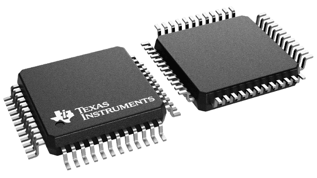
The DAC5662 is available in a 48-pin thin quad flat pack (TQFP). Pin compatibility between family members provides 12-bit (DAC5662) and 14-bit (DAC5672) resolution. Furthermore, the DAC5662 is pin compatible to the DAC2902 and AD9765 dual DACs. The device is characterized for operation over the military temperature range of -55°C to 125°C.


