| Integrated isolated power | No |
| Number of channels (#) | 3 |
| Forward/reverse channels | 2 forward / 1 reverse |
| Isolation rating (Vrms) | 5000 |
| Data rate (Max) (Mbps) | 50 |
| Rating | Automotive |
| Surge voltage capability (Vpk) | 10000 |
| Current consumption per channel (DC) (Typ) (mA) | 1 |
| Current consumption per channel (1 Mbps) (Typ) (mA) | 1.65 |
| Operating temperature range (C) | -40 to 125 |
| TI functional safety category | Functional Safety-Capable |
| Default output | High, Low |
| Supply voltage (Max) (V) | 5.5 |
| Supply voltage (Min) (V) | 1.71 |
| Propagation delay (Typ) (ns) | 11 |
- Functional Safety-Capable
- Documentation available to aid functional safety system design: ISO6731-Q1
- AEC-Q100 qualified with the following results:
- Device temperature Grade 1: –40°C to +125°C ambient operating temperature range
- Meets VDA320 isolation requirements
- 50 Mbps data rate
- Robust isolation barrier:
- High lifetime at 1500 VRMS working voltage
- Up to 5000 VRMS isolation rating
- Up to 10 kV surge capability
- ±75 kV/μs typical CMTI
- Wide supply range: 1.71 V to 1.89 V and 2.25 V to 5.5 V
- 1.71 V to 5.5 V level translation
- Default output high (ISO6731-Q1) and low (ISO6731F-Q1) options
- 1.6 mA per channel typical at 1 Mbps
- Low propagation delay: 11 ns typical
- Robust electromagnetic compatibility (EMC)
- System-level ESD, EFT, and surge immunity
- ±8 kV IEC 61000-4-2 contact discharge protection across isolation barrier
- Low emissions
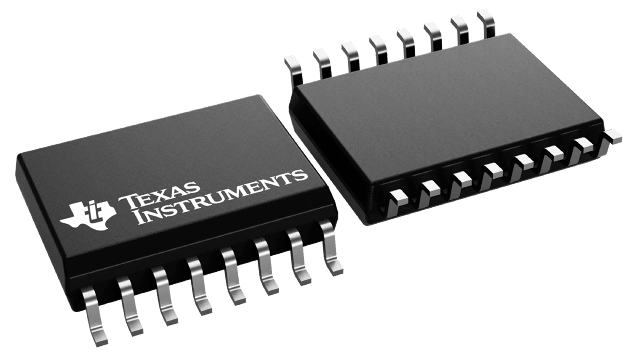
- Wide-SOIC (DW-16) Package
- Safety-Related Certifications:
- DIN VDE V 0884-11:2017-01
- UL 1577 component recognition program
- IEC 62368-1, IEC 61010-1, IEC 60601-1
- GB 4943.1-2011 certifications (pending)
The ISO6731-Q1 device is a high-performance, triple-channel digital isolators ideal for cost-sensitive applications requiring up to 5000 VRMS isolation ratings per UL 1577. This device is also certified by VDE, TUV, CSA, and CQC.
The ISO6731-Q1 devics provides high electromagnetic immunity and low emissions at low power consumption, while isolating CMOS or LVCMOS digital I/Os. Each isolation channel has a logic input and output buffer separated by TI?s double capacitive silicon dioxide (SiO2) insulation barrier. This device comes with enable pins which can be used to put the respective outputs in high impedance for multi-master driving applications. The ISO6731-Q1 device has two forward and one reverse-direction channels. In the event of input power or signal loss, the default output is high for the device without suffix F and low for the device with suffix F. See Device Functional Modes section for further details.
Used in conjunction with isolated power supplies, this device helps prevent noise currents on data buses, such as CAN and LIN from damaging sensitive circuitry. Through innovative chip design and layout techniques, the electromagnetic compatibility of the ISO6731-Q1 device has been significantly enhanced to ease system-level ESD, EFT, surge, and emissions compliance. The ISO6731-Q1 device is available in a 16-pin SOIC wide-body (DW) package and is a pin-to-pin upgrade to the older generations.


