| Number of channels (#) | 2 |
| Technology Family | LVC |
| Supply voltage (Min) (V) | 2 |
| Supply voltage (Max) (V) | 3.6 |
| Input type | Standard CMOS |
| Output type | Push-Pull |
| Clock Frequency (Max) (MHz) | 100 |
| IOL (Max) (mA) | 24 |
| IOH (Max) (mA) | -24 |
| ICC (Max) (uA) | 10 |
| Features | Balanced outputs, Very high speed (tpd 5-10ns), Over-voltage tolerant inputs |
- Qualified for Automotive Applications
- ESD Protection Exceeds 2000 V Per MIL-STD-883, Method 3015; Exceeds 200 V Using Machine Model (C = 200 pF, R = 0)
- Operates From 2 V to 3.6 V
- Inputs Accept Voltages to 5.5 V
- Max tpd of 5.2 ns at 3.3 V
- Typical VOLP (Output Ground Bounce) <0.8 V at VCC = 3.3 V, TA = 25°C
- Typical VOHV (Output VOH Undershoot) >2 V at VCC = 3.3 V, TA = 25°C
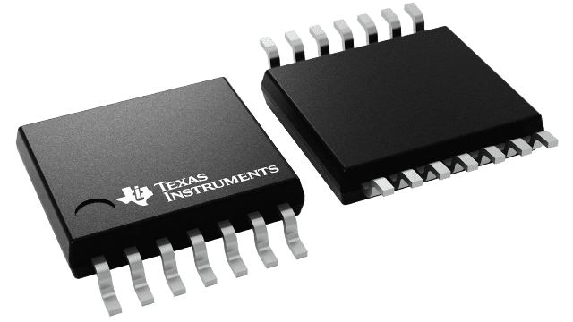
The SN74LVC74A-Q1 dual positive-edge-triggered D-type flip-flop is designed for 2.7-V to 3.6-V VCC operation.
A low level at the preset (PRE) or clear (CLR) inputs sets or resets the outputs, regardless of the levels of the other inputs. When PRE and CLR are inactive (high), data at the data (D) input meeting the setup time requirements is transferred to the outputs on the positive-going edge of the clock pulse. Clock triggering occurs at a voltage level and is not directly related to the rise time of the clock pulse. Following the hold-time interval, data at the D input can be changed without affecting the levels at the outputs.
Inputs can be driven from either 3.3-V or 5-V devices. This feature allows the use of this device as a translator in a mixed 3.3-V/5-V system environment.


