| Technology Family | CD4000 |
| Supply voltage (Min) (V) | 3 |
| Supply voltage (Max) (V) | 18 |
| Number of channels (#) | 2 |
| Inputs per channel | 2 |
| IOL (Max) (mA) | 89 |
| IOH (Max) (mA) | 0 |
| Input type | Standard CMOS |
| Output type | Open-Drain |
| Features | Standard speed (tpd > 50ns) |
| Data rate (Max) (Mbps) | 8 |
| Rating | Catalog |
- 32 times standard B-Series output current drive sinking capability - 136 mA typ. @ VDD = 10 V, VDS = 1 V
- 100% tested for quiescent current at 20 V
- Maximum input current of 1 μA at 18 V over full package-temperature range; 100 nA at 18 V and 25°C
- 5-V, 10-V, and 15-V parametric ratings
- Noise margin, full package temperature range, RL to VDD = 10 k
 :
:
???1 V at VDD = 5 V
???2 V at VDD = 10 V
???2.5 V at VDD = 15 V - Meets all requirements of JEDEC Tentative Standard No. 13B, "Standard Specifications for Description of 'B' Series CMOS Devices"
- Applications
- Driving relays, lamps, LEDs
- Line driver
- Level shifter (up or down)
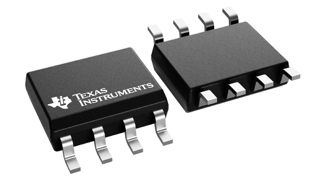
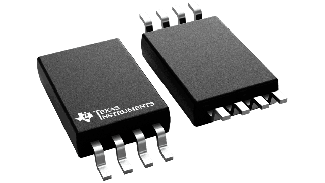
The CD40107B is a dual 2-input NAND buffer/driver containing two independent 2-input NAND buffers with open-drain single n-channel transistor outputs. This device features a wired-OR capability and high output sink current capability (136 mA typ. at VDD = 10 V, VDS= 1 V). The CD40107B is supplied in 8-lead hermetic dual-in-line ceramic packages (F3A suffix), 8-lead dual-in-line plastic packages (E suffix), 8-lead small-outline packages (M, M96, MT, and PSR suffixes), and 8-lead thin shrink small-outline packages (PW and PWR suffixes).


