| Technology Family | CD4000 |
| Supply voltage (Min) | 3 |
| Supply voltage (Max) (V) | 18 |
| Number of channels (#) | 4 |
| Inputs per channel | 2 |
| IOL (Max) (mA) | 24 |
| IOH (Max) (mA) | -24 |
| Input type | Standard CMOS |
| Output type | Push-Pull |
| Features | Standard speed (tpd > 50ns) |
| Data rate (Max) (Mbps) | 16 |
| Rating | Catalog |
| Operating temperature range (C) | -55 to 125 |
- Balanced sink and source current; approximately 4 times standard "B" drive
- Equalized delay to true and complement outputs
- 100% tested for quiescent current at 20 V
- Maximum input current of 1 μA at 18 V over full package temperature range; 100nA at 18 V and 25°C
- 5-V, 10-V, and 15-V parametric ratings
- Meets all requirements of JEDEC Tentative Standard No. 13A, "Standard Specifications for Description of ’B’ Series CMOS Devices"
- Applications:
- High current source/sink driver
- CMOS-to-DTL/TTL Converter Buffer
- Display driver
- MOS clock driver
- Resistor network driver (Ladder or weighted R)
- Buffer
- Transmission line driver
CD4041UB types are quad true/complement buffers consisting of n- and p-channel units having low channel resistance and high current (sourcing and sinking) capability. The CD4041UB is intended for use as a buffer, line-driver, or CMOS-to-TTL driver. It can be used as an ultra-low power resistor-network driver for A/D and D/A conversion, as a transmission-line driver, and in other applications where high noise immunity and low power dissipation are primary design requirements.
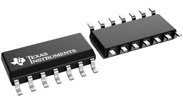
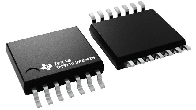
The CD4041UB types are supplied in 14-lead hermetic dual-in-line ceramic packages (F3A suffix), 14-lead dual-in-line plastic packages (E suffix), 14-lead small-outline packages (M, MT, M96, and NSR suffixes), and 14-lead thin shrink small-outline packages (PW and PWR suffixes).


