| Bus voltage (Max) (V) | 100 |
| Power switch | MOSFET |
| Input VCC (Min) (V) | 9 |
| Input VCC (Max) (V) | 14 |
| Peak output current (A) | 3 |
| Rise time (ns) | 10 |
| Operating temperature range (C) | -40 to 125 |
| Undervoltage lockout (Typ) | 8 |
| Rating | Catalog |
| Number of channels (#) | 2 |
| Fall time (ns) | 10 |
| Prop delay (ns) | 25 |
| Iq (uA) | 10 |
| Input threshold | TTL |
| Channel input logic | TTL |
| Negative voltage handling at HS pin (V) | -1 |
| Driver configuration | Dual, Independent |
- Drives Both a High-Side and Low-Side N-Channel
MOSFETs - Independent High- and Low-Driver Logic Inputs
- Bootstrap Supply Voltage up to 118 V DC
- Fast Propagation Times (25-ns Typical)
- Drives 1000-pF Load With 8-ns Rise and Fall
Times - Excellent Propagation Delay Matching (3-ns
Typical) - Supply Rail Undervoltage Lockout
- Low Power Consumption
- Pin Compatible With HIP2100/HIP2101
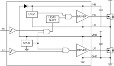
The LM5100A/B/C and LM5101A/B/C high-voltage gate drivers are designed to drive both the high-side and the low-side N-Channel MOSFETs in a synchronous buck or a half-bridge configuration. The floating high-side driver is capable of operating with supply voltages up to 100 V. The A versions provide a full 3-A of gate drive, while the B and C versions provide 2 A and 1 A, respectively. The outputs are independently controlled with CMOS input thresholds (LM5100A/B/C) or TTL input thresholds (LM5101A/B/C).
An integrated high-voltage diode is provided to charge the high-side gate drive bootstrap capacitor. A robust level shifter operates at high speed while consuming low power and providing clean level transitions from the control logic to the high-side gate driver. Undervoltage lockout is provided on both the low-side and the high-side power rails. These devices are available in the standard SOIC-8 pin, SO PowerPAD-8 pin, and the WSON-10 pin packages. The LM5100C and LM5101C are also available in MSOP-PowerPAD-8 package. The LM5101A is also available in WSON-8 pin package.


