| Configuration | 1:1 SPST |
| Number of channels (#) | 3 |
| Power supply voltage - single (V) | 0.8, 1.2, 1.8, 2.5, 3.3, 5 |
| Protocols | Analog |
| Ron (Typ) (Ohms) | 3.5 |
| CON (Typ) (pF) | 10.5 |
| ON-state leakage current (Max) (μA) | 5 |
| Bandwidth (MHz) | 100 |
| Operating temperature range (C) | -40 to 85 |
| Input/output continuous current (Max) (mA) | 64 |
| Rating | Catalog |
| Supply current (Typ) (uA) | 0.07 |
- Designed to Be Used in Voltage-Limiting Applications
- 3.5-Ω On-State Connection Between Ports A and B
- Flow-Through Pinout for Ease of Printed Circuit Board
Trace Routing - Direct Interface With GTL+ Levels
- Latch-Up Performance Exceeds 100 mA Per JESD 78,
Class II - ESD Protection Exceeds JESD 22
- 2000-V Human-Body Model
- 200-V Machine Model
- 1000-V Charged-Device Model
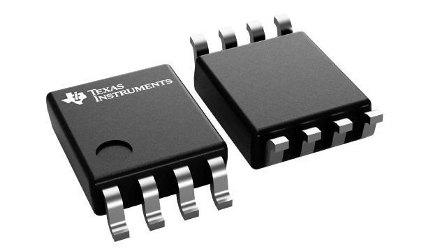
The SN74TVC3306 device provides three parallel NMOS pass transistors with a common unbuffered gate. The low on-state resistance of the switch allows connections to be made with minimal propagation delay.
The device can be used as a dual switch, with the gates cascaded together to a reference transistor. The low-voltage side of each pass transistor is limited to a voltage set by the reference transistor. This is done to protect components with inputs that are sensitive to high-state voltage-level overshoots.


