


特性
- 高输入P0.1dB: +46 dBm Tx
- 低插入损耗: 0.4 dB
- 高IIP3: +74 dBm
- 单正控制电压:
0/ +3V to 0/ +8V - 故障安全操作:
未上电时Tx为“开启” - 2x2mm DFN SMT封装
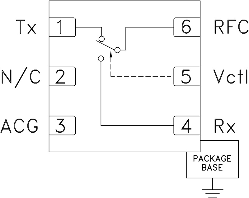
HMC646LP2(E)是一款SPDT开关,采用无引脚DFN表贴塑料封装,可用于发射/接收和LNA保护等要求极低失真和高达40 W、占空比低于10%的高功率应用。 这款鲁棒的开关可控制100 - 2100 MHz*的信号,非常适合TD-SCDMA/3G中继器、PMR、汽车远程信息处理和卫星用户终端应用。 该设计可在发射(Tx)端口提供出色的+46 dBm P0.1 dB和+74 dBm IIP3性能。 当DC电源不可用时,故障安全拓扑提供Tx到RFC的低损耗路径。
规格和数据为HMC646LP2针对数据手册中的每个指定频段使用对应的应用电路进行测量所得。
HMC646LP2ETR 应用
- LNA保护与T/R开关
- TD-SCDMA/3G基础设施
- 卫星用户终端
- 专用手机无线电与公用安全手机
- 汽车远程信息系统
Texas Instruments
ADS5525IRGZT
Analog to Digital Converters - ADCs
1-Channel Single ADC Pipelined 170Msps 12-bit Parallel/Serial/LVDS 48-Pin VQFN EP T/R
Product Technical Specifications
| EU RoHS | Compliant |
| ECCN (US) | 3A991c.2. |
| Part Status | Active |
| HTS | 8542.39.00.01 |
| Automotive | No |
| PPAP | No |
| Converter Type | General Purpose |
| Architecture | Pipelined |
| Resolution | 12bit |
| Number of ADCs | 1 |
| Number of Input Channels | 1 |
| Sampling Rate | 170Msps |
| Digital Interface Type | Parallel|Serial|LVDS |
| Input Type | Voltage |
| Input Signal Type | Differential |
| Voltage Reference | Internal|External |
| Voltage Supply Source | Analog and Digital |
| Input Voltage | 2Vp-p |
| Typical Power Dissipation (mW) | 1100 |
| Maximum Power Dissipation (mW) | 1275 |
| Integral Nonlinearity Error | ±1.6LSB |
| Full Scale Error | ±3%FSR |
| Signal to Noise Ratio | 71.2dBFS(Typ) |
| No Missing Codes (bit) | 12 |
| Sample and Hold | Yes |
| Single-Ended Input | No |
| Minimum Operating Temperature (°C) | -40 |
| Maximum Operating Temperature (°C) | 85 |
| Packaging | Tape and Reel |
| Supplier Temperature Grade | Industrial |
| Mounting | Surface Mount |
| Package Height | 0.95(Max) |
| Package Width | 7.15(Max) |
| Package Length | 7.15(Max) |
| PCB changed | 48 |
| Standard Package Name | QFN |
| Supplier Package | VQFN EP |
| Pin Count | 48 |
| Lead Shape | No Lead |