
资料下载


×
关注精确的物联网传感的ADC精密电压基准
消耗积分:0 |
格式:rar |
大小:0.45 MB |
2017-05-10
分享资料个
关注精确的物联网传感的ADC精密电压基准
最新的模拟到数字转换器(ADC)提供高性能的信号转换为广泛的应用需求。对于物联网设计,一个关键的问题仍然是一个平衡要求的精密测量的愿望,以尽量减少设计的规模和复杂性。在达到这种平衡,设计师面临着一个关键的决定,采用最有效的电压基准源的应用。集成ADC的参考电压可以简化设计,但当应用程序需要最佳的测量精度,外部参考电压电路通常是明确的选择。
准确的测量是物联网视觉的物理现象的详细分析的基础,精确的电压基准是必不可少的精确测量。不管一个ADC的底层架构,它的操作从根本上依赖于一个输入电压的比较基准电压,以创建一个适当的输出代码的基础上,这些值。在理想情况下,这种关系表示为
Output code = VIN x (2n/VREF)
where:
VIN is the analog input voltage to the ADC,
n is the number of ADC output bits, and
VREF is the analog value of the reference voltage supplied to the ADC.
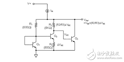
Traditional voltage reference designs are built around a bandgap reference circuit (Figure 1)。 In this conventional design, the output is produced by summing voltage components with opposite polarity temperature coefficients to produce an output voltage that is reasonably temperature-stable and equal to the silicon bandgap voltage of 1.205 V. Most voltage reference designs extend this basic design with circuitry to increase the reference voltage level and buffer the output against load changes.

声明:本文内容及配图由入驻作者撰写或者入驻合作网站授权转载。文章观点仅代表作者本人,不代表电子发烧友网立场。文章及其配图仅供工程师学习之用,如有内容侵权或者其他违规问题,请联系本站处理。 举报投诉
评论(0)
发评论
- 相关下载
- 相关文章


