
资料下载


FRAM芯片扩展在低功率应用中的耐力
分享资料个
FRAM芯片扩展在低功率应用中的耐力
虽然EEPROM和FLASH通常被用于非易失性存储器的首选(NVM)在大多数应用中,铁电存储器(FRAM)为能量收集应用如无线传感器节点,智能电表的许多低功耗设计独特的优势,和其他数据采集设计。其扩展的读写周期和数据保留时间,FRAM技术可以帮助设计人员满足要求使用十年,FRAM芯片低功耗运行框架基于MCU的NVM制造商包括Cypress半导体、富士通半导体、罗姆半导体、德克萨斯文书。
传统的NVMs,如FLASH和EEPROM,在浮栅中的电荷泵,需要提高电压的需要迫使运营商通过栅氧化层的水平电荷载体的形式存储数据。其结果是,随着长期写入延迟和高功率消耗在这些设备中固有的,其高电压写操作可以最终磨损细胞-有时在只有10000个写周期。
FRAM advantages
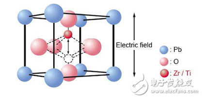
In contrast, Ferroelectric RAM (FRAM) stores data by means of the polarization of the ferroelectric material lead zirconate titanate, or PZT (Pb (ZrTi)O3), which is placed as a film between two electrodes similar to the structure of a capacitor. As with a DRAM, each bit in a FRAM array is read and written individually, but while DRAM uses a transistor and capacitor to store the bit, FRAM uses a dipole shift in the crystalline structure for the corresponding bit caused by application of an electric field across the electrodes (Figure 1)。 Because this polarization remains after the electric field is removed, the FRAM data persists indefinitely even without available power – a vital capability for designs powered by uncertain ambient sources.

声明:本文内容及配图由入驻作者撰写或者入驻合作网站授权转载。文章观点仅代表作者本人,不代表电子发烧友网立场。文章及其配图仅供工程师学习之用,如有内容侵权或者其他违规问题,请联系本站处理。 举报投诉
- 相关下载
- 相关文章


