
资料下载


RDA1846S的相关资料
分享资料个
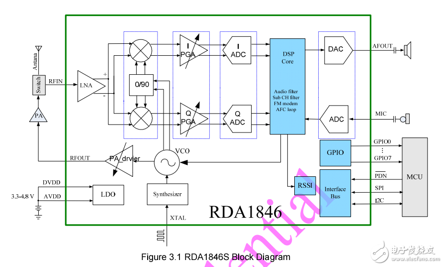
The RDA1846S transceiver features very low solution cost and reduced complexity. As shown in Fig.3.1,
to totally complete the translation from RF carrier to voice in the RX path and from voice to RF carrier in
the TX path, the chip integrates nearly all the functional blocks including RF and base band analog blocks
and digital signal processor. It requires only one micro controller and a few external components to
realize a walkie-talkie.
A powerful integrated DSP accomplishes both the demodulation and modulation of the FM signal.
Besides, standard walkie-talkie features such as CTS, CDS, VOX and SQ etc. are provided through the 8
GPIOs of the chip. Especially, by virtue of the state-of-the-art CMOS technology advanced algorithms
such as AFC, AGC, RSSI and SNR calculations are realized in the DSP, which guarantees the high
receiving and transmitting quality while still consumes a low power. Flexible RX/TX/SLEEP auto switching
function from the DSP further reduces the average power consumptions.
LDOs are also integrated in the chip which further reduces the BOMs.
All interface pins of the chip will be shortly explained below. For details, refer to the ‘RDA 1846
programming guide’。
3.1 RF input and output
The chip can receive and transmit RF signals from 400 to 500MHz and from 134 to 174MHz which cover
most of the walkie-talkie frequency bands around the world and the weather broadcast band. For the RF
input, a direct-in connection from the antenna to the LNA input pin through a switch is suggested which
means no input impedance matching is needed for the receive band. For the RF out, a pa diver can
deliver no more than 8 dBm power to PA. PA bias voltage from 1.5V~2.8V for the power amplifier can be
supplied from the PABIAS pin.

声明:本文内容及配图由入驻作者撰写或者入驻合作网站授权转载。文章观点仅代表作者本人,不代表电子发烧友网立场。文章及其配图仅供工程师学习之用,如有内容侵权或者其他违规问题,请联系本站处理。 举报投诉
-
 jf_75730806
2020-10-19
0 回复 举报学习学习,谢谢!!! 收起回复
jf_75730806
2020-10-19
0 回复 举报学习学习,谢谢!!! 收起回复
-
 7_fish
2018-07-16
0 回复 举报感谢分享,学习一下 谢谢 收起回复
7_fish
2018-07-16
0 回复 举报感谢分享,学习一下 谢谢 收起回复
- 相关下载
- 相关文章


