
资料下载


18兆位DCD同步SRAM的流水线cy7c1386d
分享资料个
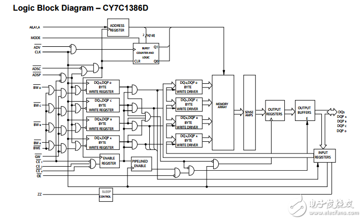
The CY7C1386D/CY7C1387D SRAM integrates 512K × 36/1M × 18 SRAM cells with advanced synchronous peripheral circuitry and a two-bit counter for internal burst operation. All synchronous inputs are gated by registers controlled by a positive edge triggered clock input (CLK)。 The synchronous inputs include all addresses, all data inputs, address-pipelining chip enable (CE1), depth expansion chip enables (CE2 and CE3), burst control inputs (ADSC, ADSP, and ADV), write enables (BWX, and BWE), and global write (GW)。 Asynchronous inputs include the output enable (OE) and the ZZ pin. Addresses and chip enables are registered at rising edge of clock when either address strobe processor (ADSP) or address strobe controller (ADSC) are active. Subsequent burst addresses can be internally generated as controlled by the advance pin (ADV)。 Address, data inputs, and write controls are registered on-chip to initiate a self timed write cycle.This part supports byte write operations (see Pin Configurations on page 5 and Truth Table on page 11 for further details)。 Write cycles can be one to four bytes wide as controlled by the byte write control inputs. GW active LOW causes all bytes to be written. This device incorporates an additional pipelined enable register which delays turning off the output buffers an additional cycle when a deselect is executed.This feature allows depth expansion without penalizing system performance. The CY7C1386D/CY7C1387D operates from a +3.3 V core power supply while all outputs operate with a +3.3 V or +2.5 V supply. All inputs and outputs are JEDEC-standard and JESD8-5-compatible. For a complete list of related documentation, click here.

声明:本文内容及配图由入驻作者撰写或者入驻合作网站授权转载。文章观点仅代表作者本人,不代表电子发烧友网立场。文章及其配图仅供工程师学习之用,如有内容侵权或者其他违规问题,请联系本站处理。 举报投诉
- 相关下载
- 相关文章


