
资料下载


2.5伏至5.5伏230微米双轨至轨输出电压的10/2位数模转换器ad5313/ad5323数据表
分享资料个
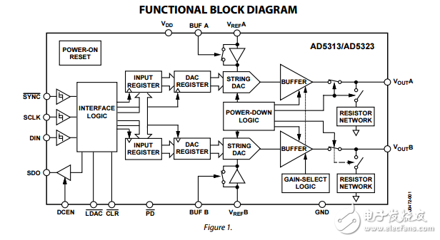
The AD5313/AD5323 are dual, 10-/12-bit buffered voltage output DACs in a 16-lead TSSOP package that operate from a single 2.5 V to 5.5 V supply, consuming 230 μA at 3 V. Their on-chip output amplifiers allow the outputs to swing rail to rail with a slew rate of 0.7 V/μs. The AD5313/AD5323 utilize a versatile 3-wire serial interface that operates at clock rates up to 30 MHz and is compatible with standard SPI, QSPI™, MICROWIRE™, and DSP interface standards. The references for the two DACs are derived from two reference pins (one per DAC)。 These reference inputs can be configured as buffered or unbuffered inputs. The devices incorporate a poweron reset circuit, which ensures that the DAC outputs power up to 0 V and remain there until a valid write to the device takes place. There is also an asynchronous active low CLR pin that clears both DACs to 0 V. The outputs of both DACs can be updated simultaneously using the asynchronous LDAC input. The devices contain a power-down feature that reduces the current consumption of the devices to 200 nA at 5 V (50 nA at 3 V) and provides software-selectable output loads while in powerdown mode. The devices can also be used in daisy-chaining applications using the SDO pin. The low power consumption of these devicesin normal operation makes them ideally suited to portable battery operated equipment. The power consumption is 1.5 mW at 5 V and 0.7 mW at 3 V, reducing to 1 μW in power-down mode.

声明:本文内容及配图由入驻作者撰写或者入驻合作网站授权转载。文章观点仅代表作者本人,不代表电子发烧友网立场。文章及其配图仅供工程师学习之用,如有内容侵权或者其他违规问题,请联系本站处理。 举报投诉
- 相关下载
- 相关文章


