
资料下载


16/14/12位SPI纳米DAC和2 LSB INL理论参考ad5683r/ad5682r/ad5681r/ad5683数据表
分享资料个
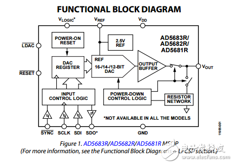
The AD5683R/AD5682R/AD5681R/AD5683, members of the nanoDAC+® family, are low power, single-channel, 16-/14-/12-bit buffered voltage out digital-to-analog converters (DACs)。 The devices, except the AD5683, include an enabled by default internal 2.5 V reference, offering 2 ppm/°C drift. The output span can be programmed to be 0 V to VREF or 0 V to 2 × VREF. All devices operate from a single 2.7 V to 5.5 V supply and are guaranteed monotonic by design. The devices are available in a 2.00 mm × 2.00 mm, 8-lead LFCSP or a 10-lead MSOP. The internal power-on reset circuit ensures that the DAC register is written to zero scale at power-up while the internal output buffer is configured in normal mode. The AD5683R/AD5682R /AD5681R/AD5683 contain a power-down mode that reduces the current consumption of the device to 2 µA (maximum) at 5 V and provides software selectable output loads while in powerdown mode. The AD5683R/AD5682R/AD5681R/AD5683 use a versatile 3-wire serial interface that operates at clock rates of up to 50 MHz. Some devices also include asynchronous RESET pin and VLOGIC pin options, allowing 1.8 V compatibility.

声明:本文内容及配图由入驻作者撰写或者入驻合作网站授权转载。文章观点仅代表作者本人,不代表电子发烧友网立场。文章及其配图仅供工程师学习之用,如有内容侵权或者其他违规问题,请联系本站处理。 举报投诉
- 相关下载
- 相关文章


