
资料下载


低电容16和8通道多路复用器CMOS工艺ADG1206/ADG1207数据表
分享资料个
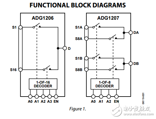
The ADG1206 and ADG1207 are monolithic iCMOS® analog multiplexers comprising sixteen single channels and eight differential channels, respectively. The ADG1206 switches one of sixteen inputs to a common output, as determined by the 4-bit binary address lines A0, A1, A2, and A3. The ADG1207 switches one of eight differential inputs to a common differential output, as determined by the 3-bit binary address lines A0, A1, and A2. An EN input on both devices is used to enable or disable the device. When disabled, all channels are switched off. When on, each channel conducts equally well in both directions and has an input signal range that extends to the supplies. The industrial CMOS (iCMOS) modular manufacturing process combines high voltage, complementary metal-oxide semiconductor (CMOS) and bipolar technologies. It enables the development of a wide range of high performance analog ICs capable of 33 V operation in a footprint that no other generation of high voltage devices has been able to achieve. Unlike analog ICs using conventional CMOS processes, iCMOS components can tolerate high supply voltages while providing increased performance, dramatically lower power consumption, and reduced package size. The ultralow capacitance and exceptionally low charge injection of these multiplexers make them ideal solutions for data acquisition and sample-and-hold applications, where low glitch and fast settling are required. Figure 2 shows that there is minimum charge injection over the entire signal range of the device. iCMOS construction also ensures ultralow power dissipation, making the devices ideally suited for portable and batterypowered instruments.

声明:本文内容及配图由入驻作者撰写或者入驻合作网站授权转载。文章观点仅代表作者本人,不代表电子发烧友网立场。文章及其配图仅供工程师学习之用,如有内容侵权或者其他违规问题,请联系本站处理。 举报投诉
- 相关下载
- 相关文章


