资料下载

Packaging Innovation Enables Power Efficiency for Wearables
Packaging Innovation Enables Power Efficiency for Wearables
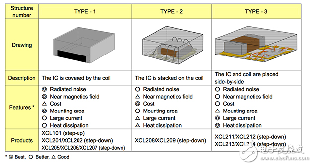
对于可穿戴设备,小尺寸是组件选择的一个重要因素,包括那些用于电源。直流/直流转换器的出现,都可以提供高转换效率,同时最大限度地减少电路板空间整合转换控制器及关键无源器件到系统封装模块,有助于减少尺寸和简化的布局。本文着眼于包装一体化有助于降低开关的服饰和设计方面的考虑在处理这些设备器尺寸的方法。
可穿戴设备的设计提出了一些挑战,但其中一个关键因素是电源效率,不仅在能源方面,但规模。这些器件磨损了很长一段时间,所以他们需要良好的电池自主性。他们接近皮肤也需要高效率的转换器,可以通过开关电源提供的东西,而不是传统的低压差稳压器,已在过去的紧凑性青睐。然而,开关模式的设计更复杂。

Although CMOS integration has allowed the scaling down of active components that include on-chip power transistors, traditional DC/DC converter designs assume the use of external passive components. These individual devices may not consume much volume on their own, but when used in combination to support the operation of the converter, require significant board space compared to the primary SoC.
Larger portable designs have been able to tolerate the board space required by the power circuitry. However, wearables by nature of their smaller size and demand for as much battery volume as possible for maximum time between charges put intense pressure on the other components in the system in terms of space.
声明:本文内容及配图由入驻作者撰写或者入驻合作网站授权转载。文章观点仅代表作者本人,不代表电子发烧友网立场。文章及其配图仅供工程师学习之用,如有内容侵权或者其他违规问题,请联系本站处理。 举报投诉
- 相关下载
- 相关文章


